
ADC6000
40 GSa/s, 8-Bit
- High-speed waveform digitizer with built-in processing hardware and fast data transfer to external computer
- Up-to 13 GHz analog bandwidth of 8-bit A/D Converter with 40 GSa/s sampling rate in 1 channel mode
- Up-to 128 GBytes of acquisition memory per module. Total of 1.66 TByte of acquisition memory available in 14 slot AXIe-1 chassis
- Digital hardware-accelerated frequency response equalization, with custom programming capability
- FPGA-based reconfigurable digital signal processing with up to 10 GSa/s processing speed
- Multiple Firmware options available to accelerate measurements
- High-speed data transfer to host computer and graphic processors (GPU) for fast signal processing
- Up to 1.6 GByte/s data transfer rate to computer using PCI Express x4 Gen 2 link
- 1U AXIe module 200 Watt maximum power consumption
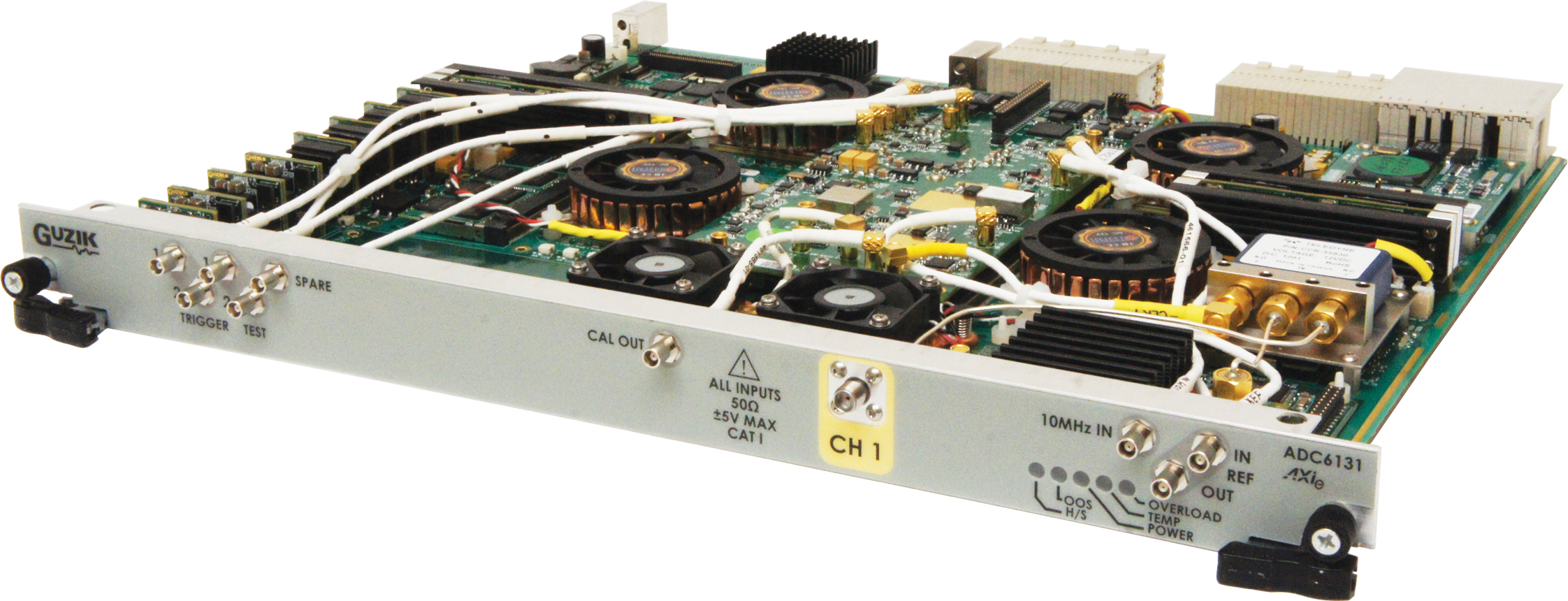
Guzik AXIe ADC 6000 Series Digital Acquisition and Processing Modules combine high-speed waveform digitizer with built-in digital signal processing hardware, which enables mixed-domain signal capture and analysis with high-speed data transfer link to a computer. The ADC 6000 Modules come in a space-saving display-less 1U 19” AXIe modular form factor.
The product addresses demanding ATE and OEM systems applications in semiconductors, military electronics, physics, astronomy, avionics, and a variety of other disciplines, as well as the disk drive head and media testing applications.
The waveform digitizer ADC 6000 series modules feature Keysight A/D converters with sampling rates up to 40 GSa/s and analog bandwidth up to 13 GHz. ADC 6000 with up-to 128 GBytes of acquisition memory delivers the longest waveform capture time window available in a high bandwidth analog to digital converter instrument.
ADC 6000 features an FPGA-based reconfigurable digital signal processor with up to 10 GSa/s combined processing speed to convey massive time-critical computations directly inside the instrument.
The PCI Express Gen. 2 link provides fast DMA transfer of the acquired data to the host computer’s GPU and CPU-based processing back-end. The x4 link delivers 1.6 GByte/s sustained data transfer rate.
A Software Development Kit is supplied to control the instrument and to integrate the ADC 6000 into an existing AXIe measurement system. Guzik also supplies Signal Display soft front panel graphical interface application for signal capturing and visualization.
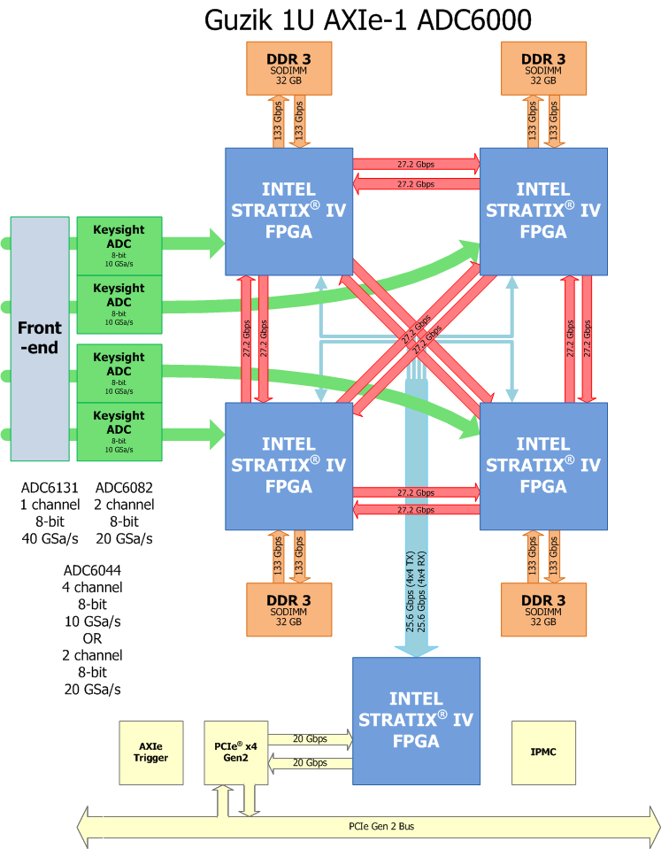
The block diagram below shows the main components of ADC 6000 in an AXIe system in four-channel configuration:
Figure 1. Block diagram of four-channel ADC 6000 in standard Keysight AXIe chassis
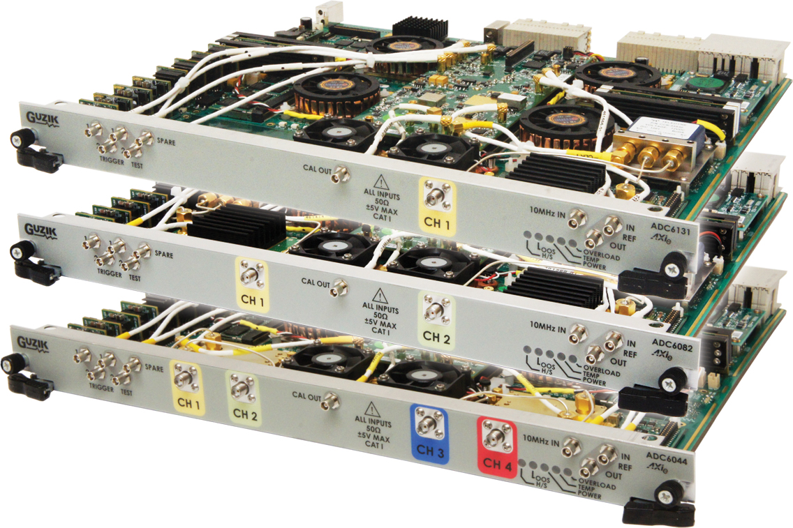
Guzik AXIe Digitizer Modules
ADC 6000 Series includes three modules listed in the table below:
| ADC 6131 | ADC 6082 | ADC 6044 | |
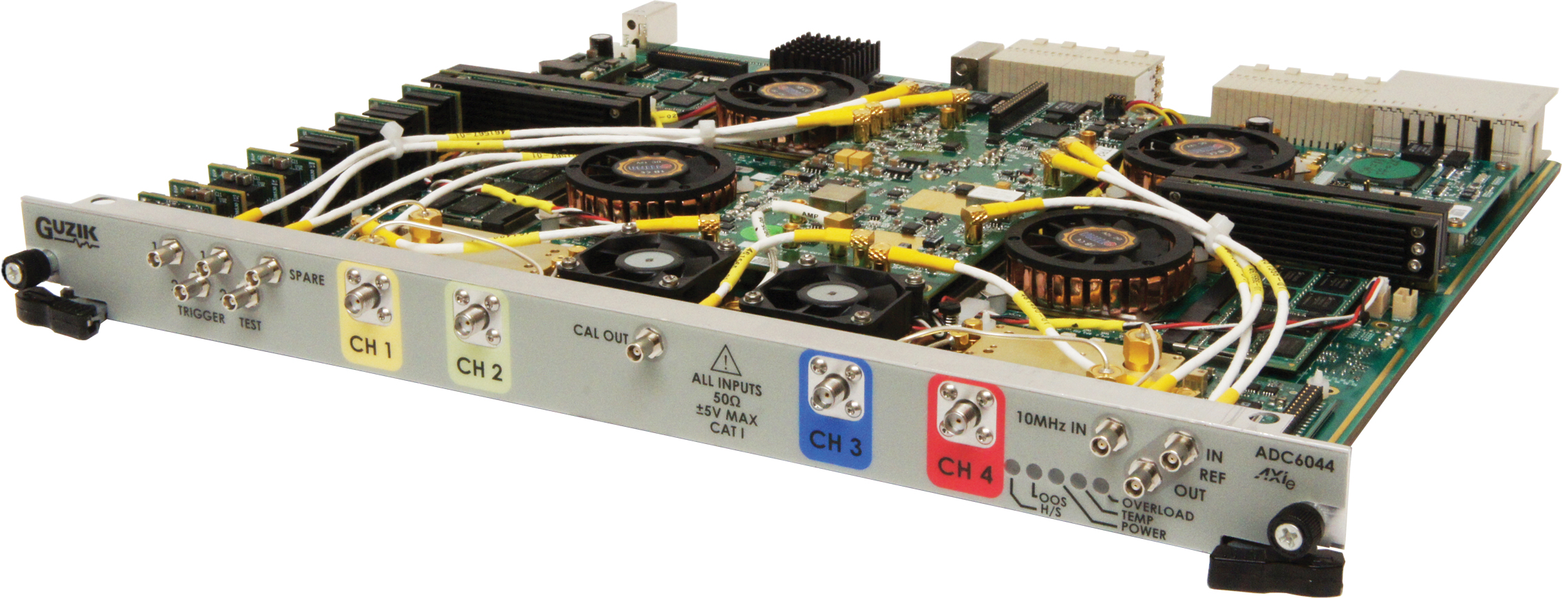
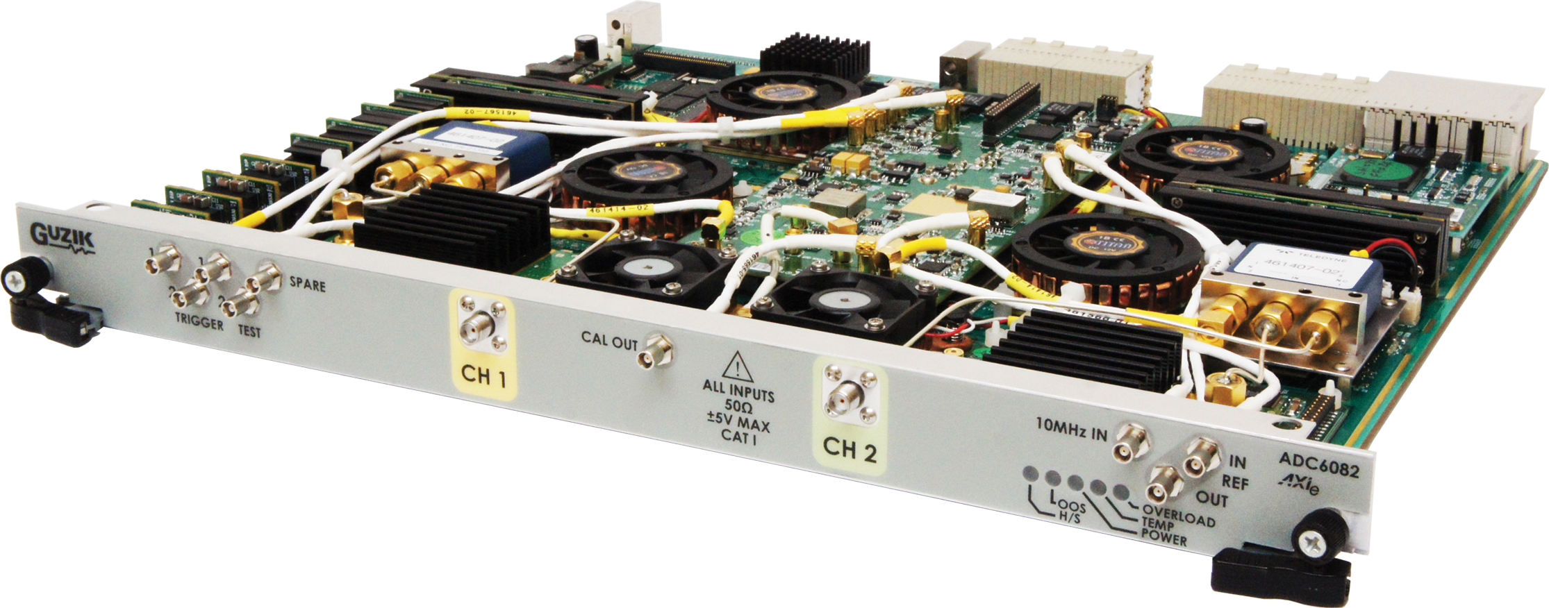
| Input Channels | 1 | 2 | 4 |
| Analog Bandwidth (-3db) |
13 GHz | 8 GHz | 6.5 GHz (2-ch mode)4 GHz (4-ch mode) |
| Sampling Rate (per channel) |
40 GSa/s | 20 GSa/s | 20 GSa/s (2-ch mode)10 GSa/s (4-ch mode) |
| Acquisition Memory1 (per channel maximum) |
120 GSa | 60 GSa | 60 GSa (2-ch mode)30 GSa (4-ch mode) |
| PCI Express Gen 2 Interface to computer | x4 standard | x4 standard | x4 standard |
________________
1 With 15/16 memory utilization
Acquisition System
At the heart of the ADC 6000 Digitizer Modules are state of the art high-speed real-time analog to digital converter ASICs supplied by Keysight Technologies, which provide high speed waveform capture. The patented2 Guzik digital hardware-accelerated frequency response equalization further improves the signal fidelity and effective number of bits.
At the maximum sampling rate of 40 GSa/s (25 psec per point), the ADC 6000 can capture up to 3.2 seconds of a real-time waveform into its ultra-long acquisition memory –
128 GBytes for single channel configuration.
________________
2 U.S. Patent 7,408,495
Trigger
The ADC 6000 features a digital processing trigger. This feature makes use of the real-time hardware waveform processing capability and allows you to define trigger parameters based on the actual digital waveform data. This trigger is available on any input channel. In addition one of two external trigger/gate source inputs is provided. Trigger conditions are set using the Signal Display software tool or from your application via SDK.
External Clock and I/O

The ADC 6000 Modules feature 50 ohm SMA connectors for inputs and MCX connectors for external trigger and control I/O connections.
One 10 MHz input and one 50MHz reference clock input. One 50MHz reference clock output from the digitizer is available to allow precise time base synchronization with more than one digitizer, oscilloscope, RF instruments or logic analyzers. Optionally a 1GHz reference clock connection can be made available instead of the internal ADC clock, by configuring the SPARE connector on the front panel as an input.
Several test outputs are available for custom application support and system integration.
ADC 6000 provides a programmable calibrator output with a variety of test signals. The calibrator could be connected to any input channel and run an automatic calibration routine to ensure accurate operation of the instrument. The calibrator feature is a special-configuration. Please contact Guzik Technical Enterprises for more information.
PCI Express Host Computer Interface
 The ADC 6000 provides PCI Express Gen 2 x4 interface to the AXIe backplane. The PCI Express bridge card installs into the host computer, and a standard PCI Express x8 cable connects the AXIe chassis to the host computer. High speed waveform transfer with sustained data rates up to 1.6 GByte/sec is possible from this port back to the host computer.
Processing Overview and Capabilities
ADC 6000 provides various options for signal processing: FPGA, GPU, and CPU-based processing.
FPGA-based Processing
Inside the ADC 6000 are four Altera StratixTM IV FPGA’s. These core processing elements combined with Guzik’s implementation of customer-specified measurement algorithms provide end users with a truly tailored measurement solution where speed and throughput count. 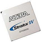
The FPGA-based processor combined with Guzik’s custom engineering capabilities provides you with the possibility to perform digital signal processing directly in ADC 6000 prior to sending waveform data out to computer. Many applications may require only processed results to be sent to the host computer rather than raw waveform data. Guzik can work directly with customers to implement custom processing capabilities drawing from years of experience in waveform analysis. Choice of firmware options includes channel equalization, filtering, multi-segment time-tagged acquisition, Digital Down Conversion (DDC), Fast Fourier Transform (FFT), Discrete Fourier Transform (DFT), min/max, real-time averaging, and parameter calculations among others are all available along with application-specific requests. Guzik can provide custom services after a technical consultation regarding the specific application and required processing.
The combined FPGA processing resources are listed in the table below:
| Processing Block | Number | Notes |
| Logic Cells | 729,600 | 1 LUT and 1 flip-flop |
| Block RAM |
4,940 88 |
9-Kbit blocks 144-Kbit blocks |
| Multipliers | 5,152 | 18-bit x 18-bit multipliers |
Information about the ADC 6000 available options:
| Firmware Option | Description |
|
ADC_BASE (Digitizer Base License) |
Base license for one segment simultaneous acquisition and readout of data to the host computer, with patented6 digital Time-Interleaved ADC mismatch, frequency response and phase equalization. See white paper Equalization of Multiple Interleaved Analog-to-Digital Converters (ADCs) |
|
ADC_SM (Segmented Memory Acquisition) |
Multi segment acquisitions in the Guzik digitizers use a circular acquisition buffer with minimum inter-segment dead-time of 300ns. This allows, for example, to capture up to 64 million repetitive signals with relatively large repetition intervals and better utilize the already large acquisition memory by discarding dead-time in between signals. Down to femtosecond resolution time-tagging allows to know the precise time between each captured waveform segment. Please refer to GSA SDK User’s Guide section 5.1.2 Acquisition Format Specification |
|
ADC_BB (Low-pass filtering and decimation) |
Digital low-pass filter (LPF) is used to reduce the analog bandwidth of the digitizer. It has an adjustable bandwidth of 6.5 GHz and down to 125 MHz. If the input signal bandwidth is lower than the digitizer’s analog bandwidth, then a filter with a lower cutoff frequency can be applied to improve SNR and ENOB. Since the cutoff frequency is lowered, decimation by powers of 2 is performed. Decimation reduces sampling rate, therefore reduces the data speed to store data to the onboard memory and to transfer data to the host computer. It also extends the acquisition time proportional to the decimation factor. |
|
ADC_BBRT1 (Real-Time 10 GSa/s Baseband Filtering) |
To increase acquisition time for longer signals, which have smaller analog bandwidth than the digitizer, the Real-time 10 GSa/s baseband digital filtering and decimation option can be used to reduce acquisition data and increase ENOB before storing it to the memory. This option enables triggered streaming and recording of up to aggregated 1.25 GSa/s or 500MHz of baseband with the ADC6044 across all channels together with the segmented memory option. Trigger/gate resampled at 250 MHz. Please refer to GSA SDK User’s Guide section 5.7 Performing Data Streaming |
|
ADC_DDC (Digital Down Converting) |
In Guzik digitizers the Digital Down Conversion DDC is implemented using FPGAs. The data from ADC is transferred to the memory and from memory through digital equalizer to DDC. The down conversion is implemented by two multipliers with Sin/Cos LO signals. Down converted signals are connected through LPF/decimator to I/Q memory and transferred to PC. Keysight 89600 VSA software can be used to tune each digitizer channel center frequency independently and can perform final processing and measurements related to particular transmission standard for measurement channels simultaneously. This method significantly reduces the amount of data transferred to PC and in return increases measurement speeds. Please refer to GSA SDK User’s Guide section 5.8 Performing Digital Down Conversion |
|
ADC_DDCRT1 (Real-Time 10 GSa/s Digital Down Converting) |
The Real-Time 10 GSa/s Digital Down Conversion option allows to perform the down conversion in real-time in the ADC6044 digitizer FPGAs. Real-time IF Magnitude triggering can be used to decide if data is to be stored to the digitizer I/Q memory or not. This allows to capture and store only signals of interest within the DDC span and reduces the data amount needed to be transferred to the PC for post processing. Keysight 89600 VSA software can be used to tune each digitizer channel center frequency independently and can perform final processing and measurements related to particular transmission standard for measurement channels simultaneously. Please refer to GSA SDK User’s Guide section 5.9 Performing Digital Down Conversion in Real Time |
|
ADC_AVG (High Speed Deep Averaging) |
Averaging for noise reduction is used in measurements when high dynamic range is required. Averaging is done in real-time in FPGAs thousands of times faster compared to other methods. With the 40-bit 640K internal accumulator the accuracy of measurements is greatly increased by allowing up-to 4 billion averaged waveforms. This allows viewing side bands spectral regrowth and other repetitive signals previously hidden in the noise. Please refer to GSA SDK User’s Guide section 5.6 Performing Real Time Accumulation Measurement |
| ADC_AVGS (Bundles ADC_SM and ADC_AVG)(High Speed Deep Segmented Averaging) |
Segmented averaging mode further advances the measurement flexibility by utilizing groups of data of interest into segments. Each segment may either have its own trigger event programmed or just suspend the data accumulation process for specified period of time. Please refer to GSA SDK User’s Guide section 5.6 Performing Real Time Accumulation Measurement |
|
ADC_M128 (128 GByte Acquisition Memory Option) |
Capture the longest time spans at full sample rate with an acquisition memory upgrade to 128 GByte. Longer time capture at full sample rate provides superior acquisitions to hunt down those difficult to find problems in applications with mixed analog and digital signals, serial busses, or various communication signals. Please refer to GSA SDK User’s Guide section 4.4.3.1 Input Resources Configuration |
|
ADC_SYNC1 (Multi-Module Synchronization Capability) |
Multi-module synchronization capability, allows to increase the total number of digitizer channels by combining multiple modules into one instrument. The new option enables multichannel phase coherent time-tagged input channels to be triggered from common source or independently. Synchronization is performed during digitizer initialization and channel-to-channel skew is restored between instrument channels. The digitizers can be setup to follow an external 10 MHz or 50 MHz time base without uncertainty, which is critical for ATE and OEM systems application. Please refer to GSA SDK User’s Guide section 4.5 Synchronization of Several Digitizers and 5.1.17 Synchronous Acquisition |
________________
3 U.S. Patent 7,408,495
GPU-based Processing
 General-purpose computation on graphic hardware allows developers to reuse the computational algorithms available for GPU or develop their own algorithms on CUDA C or OpenCL. ADC 6000 is optionally shipped with NVidia® GeForce GTX 7704 GPU. It is possible to use any NVidia® GPU with computing capability 2.0 or higher, if its power requirements are satisfied by the host computer power supply.
________________
4 Current configuration. More powerful GPU cards may be shipped in the future
CPU-based Processing
In addition to FPGA-based and GPU-based computation, customers have an option to perform signal processing using a computer CPU.  Multi-core processing libraries, such as OpenMP, allow utilizing full power of modern 12-core CPU computers. Once more powerful computers with additional cores are released, you can upgrade your computer keeping your existing ADC 6000 Digitizer Module.
Ultra-fast GPU-based FFT Measurements5
ADC 6000 performs frequency domain analysis using the Fast Fourier Transform (FFT) performed on GPU. Single NVIDIA® Tesla GPU card performs FFT calculations at a 2.5 GSa/s processing speed. This means, for example, that if you collect data at 10 GSa/s for 100 µs, process in 400 µs, you will get the full signal spectrum up to 5 GHz with resolution bandwidth 10 kHz – 500,000 spectral lines – in less than 0.5 ms.
________________
5 Available using the GSA Software Development Kit (SDK)
Temperature Stabilization
The ADC 6000 digitizer modules keep constant temperature for the critical A-to-D components for better measurement accuracy. Tested at ambient temperatures from 14 C to 34 C in Guzik GSA 6000 stand-alone chassis.
ADC 6000 Modules Designed for AXIe-1 Standard
The 1U AXIe ADC 6000 Digitizer Modules install into an industry standard AXIe-1 chassis together with other instruments, such as Keysight M8190A 12 GSa/s, M8195A 65GSa/s Arbitrary Waveform Generator, and other AXIe-0 or AXIe-1 modular instruments. 
Signal Connection and Probing
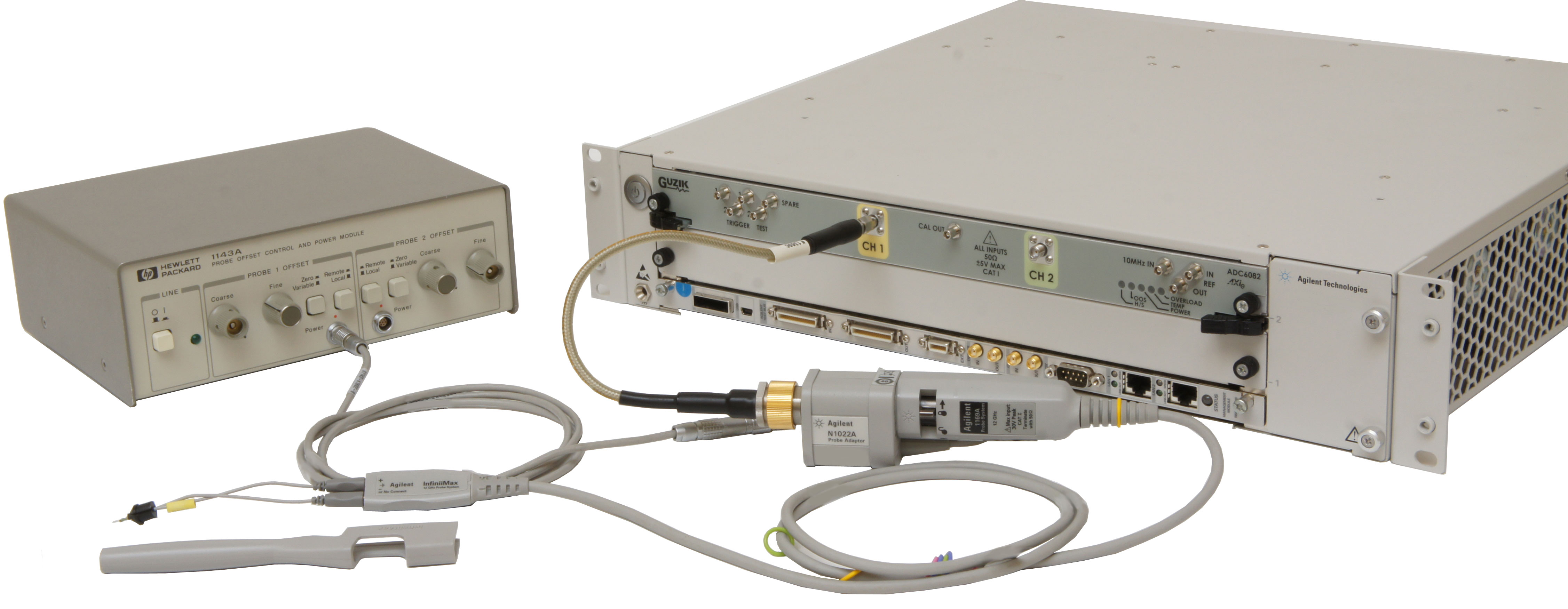
 For applications that require single ended or differential probing, Guzik recommends the Keysight InfiniiMax series of probing tools for use with the ADC 6000 digitizer Modules. Detailed selection information can be found at the following link: http://www.keysight.com/find/probes document 5968-7141EN. A wide variety of probe solutions up to 13 GHz in bandwidth can be purchased directly from Keysight.
The Keysight InfiniiMax Series6 features a variety of probe amplifier and body styles.
The interface to the ADC 6000’s input connector is the Keysight N1022B Probe Adapter, the 1143A Probe Offset Control and Power Module with an additional ruggedized 3.5 mm to SMA cable pictured below.
________________
6 Keysight and InfiniiMax are registered trademarks of Keysight, Inc.
GSA Toolkit Software
Guzik provides a GSA Toolkit to control the ADC 6000 Digitizer Modules, which includes two software components:
- GSA SDK – software development kit to create your custom standalone applications for ADC 6000 or to integrate ADC 6000 into your existing software environment; please refer to “Guzik Signal Analyzer Software Development Kit User’s Guide” document P/N 02-107544 for more details.
- Signal Display application designed for easy instrument setup, waveform acquisition and visualization. Signal Display provides oscilloscope-like graphical user interface to display multiple signal waveforms, frequency spectrum, control acquisition parameters (sampling rate, duration, trigger settings, etc), and perform multiple trigger (multi-sector) acquisitions. The application allows for saving acquired signals to files for importing into Keysight N8900A InfiniiView PC-based oscilloscope analysis software, Keysight 89600 VSA software, EXCEL, MATLAB or other computational and analysis programs. You can load and display signals from files in various formats, including the previously saved waveforms. One of the useful features of Signal Display is tracking (monitoring) acquired signals during GSA SDK-based application execution. Please refer to “Signal Display User’s Guide” document P/N 02-107548 for more details.
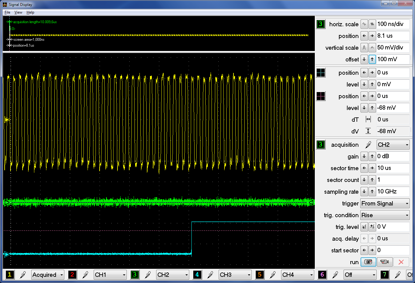
Figure 2. Signal Display Application
Specifications7
| Vertical System ADC 6044 | 2 Channel Mode |
4 Channel Mode | ||||
| Input Channels | 2, SMA Female | 4, SMA Female | ||||
| Analog Bandwidth (-3db)1,2 | 6.5 GHz | 4 GHz | ||||
| Vertical Resolution | 8 bits | |||||
| Input Impedance | 50 ohm ± 3% | |||||
| Input Coupling | DC | |||||
| Maximum Input Voltage | ± 5 V | |||||
| Input Sensitivity | 40 mV … 8 V (Full Scale) | |||||
| Bandwidth Flatness 1,2 (-6 dBFs) |
± 0.5 dB to 5 GHz -3 dB at 6.5 GHz |
± 0.5 dB to 3.5 GHz -3 dB at 4 GHz |
||||
| Effective Bits 1 (-3 dBFs, 400 mV Full Scale) |
Frequency 100 MHz |
5.5 |
5.7 |
|||
| Rise / Fall Time (10-90%) | 68 ps | 104 ps | ||||
| RMS Noise Floor 1 |
Sensitivity (Full Scale) 40 mV |
410 uV |
241 uV |
|||
| Spurious Free Dynamic Range (SFDR) 1 (-3 dBFs, 400 mV Full Scale) |
Frequency 100 MHz |
44 dBc |
45 dBc |
|||
| DC Gain Accuracy | ± 2% of full scale at full resolution channel scale (± 2.5% for 40 mV Full Scale) |
|||||
| Offset Range |
Vertical Sensitivity (Full Scale) 0 …120 mV |
Available Vertical Offset ± 0.30 V |
||||
| Offset Accuracy |
Offset Range TBD |
TBD |
||||
| Typical Channel to Channel Isolation (any two channels with equal Vertical settings) |
Frequency < 2 GHz |
55dB |
55dB |
|||
| Return Loss | < -12 dB to 4 GHz | < -12 dB to 6 GHz | ||||
| Acquisition System ADC 6044 | 2 Channel Mode |
4 Channel Mode |
| Maximum Real Time Sample Rate | 20 GSa/s | 10 GSa/s |
| Memory Depth per Channel maximum | 64 GBytes | 32 GBytes |
| Maximum Acquired Time per Channel at Highest Real Time Sample Rate |
3.2 seconds | |
| Vertical System ADC 6082 | 2 Channels | ||
| Input Channels | 2, SMA Female | ||
| Analog Bandwidth (-3db) 1,2 | 8 GHz | ||
| Vertical Resolution | 8 bits | ||
| Input Impedance | 50 ohm ± 3% | ||
| Input Coupling | DC | ||
| Maximum Input Voltage | ± 5 V | ||
| Input Sensitivity | 40 mV … 8 V (Full Scale) | ||
| Bandwidth Flatness 1,2 (-6 dBFs) |
± 0.5 dB to 6 GHz -3 dB at 8 GHz |
||
| Effective Bits 1 (-3 dBFs, 400 mV Full Scale) |
Frequency 100 MHz |
6.0 |
|
| Rise / Fall Time (10-90%) | 49 ps | ||
| RMS Noise Floor 1 | Sensitivity (Full Scale)40 mV 80 mV 160 mV 400 mV 800 mV 1.6 V 4 V 8 V |
315 uV 400 uV 580 uV 1.60 mV 3.10 mV 6.00 mV 17.0 mV 32.5 mV |
|
| Spurious Free Dynamic Range (SFDR) 1 (-3 dBFs, 400 mV Full Scale) |
Frequency 100 MHz |
52 dBc |
|
| DC Gain Accuracy | ± 2% of full scale at full resolution channel scale (± 2.5% for 40 mV Full Scale) |
||
| Offset Range | Vertical Sensitivity (Full Scale)0 …358 mV > 358 … 637 mV > 637 …1133 mV > 1133 … 2015 mV > 2015 mV |
Available Vertical Offset
± 0.40 V |
|
| Offset Accuracy |
Offset Range TBD |
TBD |
|
| Typical Channel to Channel Isolation (any two channels with equal Vertical settings) |
Frequency < 8 GHz |
48dB |
|
| Return Loss | < -14 dB to 8 GHz | ||
Acquisition System ADC 6082 |
|
| Maximum Real Time Sample Rate | 20 GSa/s |
| Memory Depth per Channel maximum | 64 GBytes |
| Maximum Acquired Time per Channel at Highest Real Time Sample Rate |
3.2 seconds |
| Vertical System ADC 6131 | 1 Channel | ||
| Input Channels | 1, SMA Female | ||
| Analog Bandwidth (-3db) 1,2 | 13 GHz | ||
| Vertical Resolution | 8 bits | ||
| Input Impedance | 50 ohm ± 3% | ||
| Input Coupling | DC | ||
| Maximum Input Voltage | ± 5 V | ||
| Input Sensitivity | 40 mV … 8 V (Full Scale) | ||
| Bandwidth Flatness 1,2 (-6 dBFs) |
± 0.5 dB to 10 GHz -3 dB at 13 GHz |
||
| Effective Bits 1 (-3 dBFs, 400 mV Full Scale) |
Frequency 100 MHz |
5.6 |
|
| Rise / Fall Time (10-90%) | 32 ps | ||
| RMS Noise Floor 1 |
Sensitivity (Full Scale) 40 mV |
485 uV 550 uV 670 uV 2.10 mV 3.80 mV 7.40 mV 21.6 mV 45.8 mV |
|
| Spurious Free Dynamic Range (SFDR) 1 (-3 dBFs, 400 mV Full Scale) |
Frequency 100 MHz |
52 dBc |
|
| DC Gain Accuracy | ± 2% of full scale at full resolution channel scale (± 2.5% for 40 mV Full Scale) |
||
| Offset Range |
Vertical Sensitivity (Full Scale) 0 …358 mV |
Available Vertical Offset ± 0.40 V |
|
| Offset Accuracy |
Offset Range TBD |
TBD |
|
| Typical Channel to Channel Isolation (any two channels with equal Vertical settings) |
N/A | ||
| Return Loss | < -12 dB to 12.5 GHz | ||
| Acquisition System ADC6131 | |
| Maximum Real Time Sample Rate | 40 GSa/s |
| Memory Depth per Channel maximum | 128 GBytes |
| Maximum Acquired Time per Channel at Highest Real Time Sample Rate |
3.2 seconds |
| Trigger | ||
| Trigger Types |
Internal digital edge trigger on an input channel External edge trigger/gate resampled at 250 MHz |
|
|
External Trigger/Gate Input (TRIGGER 1, 2) |
Impedance |
2, MCX Female 50 Ohm |
| Control Signal Connections | ||
|
Calibrator Output (CAL OUT) |
Impedance |
1, MCX Female 50 Ohm |
|
External 10 MHz Reference Input (10 MHz IN) |
Level Impedance Coupling Stability |
1, MCX Female 0 to +10 dBm |
|
External 50 MHz Reference Input (REF IN) |
Level Impedance Coupling Stability |
1, MCX Female 0 to +10 dBm |
|
External 50 MHz Reference Output (REF OUT) |
Level Impedance Coupling |
1, MCX Female 800 mV p/p nominal |
|
External 1 GHz Clock Input (Configured optionally instead of SPARE) |
Level Impedance Coupling Stability |
1, MCX Female 0 to +10 dBm |
|
Test Outputs (TEST 1, 2) |
Level |
2, MCX Female LV TTL |
|
Spare (SPARE) |
1, MCX Female | |
| Host Computer | |
| Transfer Interface | One PCI-Express x8 Generation 2 slot |
| Transfer Speed from PC to chassis | Up-to 3.2 GByte/s via PCI-Express x8 Generation 2 link from PC to AXIe-1 chassis. |
| Transfer Speed from chassis to module | Up-to 1.6 GByte/s via PCI-Express x4 Generation 2 link to AXIe-1 module. |
| Operating System |
32-bit or 64-bit Windows 7 Linux/Windows Hybrid Configuration supported. |
| Module Physical | |
| Weight | 5.1 lbs / 2.3 kg |
| Power | 200 Watt Max |
| Operating Temperature Range | +5 C to +40 C |
| Non-Operating Temperature | -40 C to +70 C |
| Operating Altitude | Up to 4,000 meters (12,000 feet) |
| Non-Operating Altitude | Up to 15,300 meters (50,000 feet) |
________________
1 With digital equalization.
2 6-pole Butterworth approximation.
7 Specification values are typical. Specifications are subject to change.
| Hardware Base Modules: | P/N | Price | Typical Lead Time |
|
| ADC 6044, 64 GByte AXIe Digitizer Module with “basic” software |
S90-620173-XX | Call | 8-12 weeks | |
| ADC 6082, 64 GByte AXIe Digitizer Module with “basic” software |
S90-620185-XX | Call | 8-12 weeks | |
| ADC 6131, 64 GByte AXIe Digitizer Module with “basic” software |
S90-620186-XX | Call | 8-12 weeks | |
| Hardware Options: | ||||
| 128 GByte Memory Upgrade | S95-990462-XX | Call | 8-12 weeks | |
| Master Low Phase Noise 50 ppb time base upgrade | S95-990463-XX | Call | 8-12 weeks | |
| Firmware Options: | ||||
| ADC_BASE | Included with base module | |||
| ADC_SM | S87-777623-XX | Call | Available | |
| ADC_BB | S87-777624-XX | Call | Available | |
| ADC_AVGS (Includes ADC_SM and ADC_AVG) | S87-777625-XX | Call | Available | |
| ADC_AVG | S87-777618-XX | Call | Available | |
| ADC_DDC | S87-777626-XX | Call | Available | |
| ADC_M128 (Requires 128 GByte hardware upgrade) | S87-777629-XX | Call | Available | |
| Multi-module Configuration | Call | Call | ||
| Accessories: | ||||
| Guzik x8 PCIe Gen2 Bridge Card to connect AXIe chassis to the host PC |
S60-705574-XX | Call | Available | |
| x8 PCIe Gen2 Two Meter Cable Assembly | S30-109656-XX | Call | Available | |
| Software Packages | ||||
|
“Basic” software package includes: · GSA SDK APIs: Acquisition Sample code (C++, Matlab) · Signal Display Soft Front Panel |
||||
![]() Product Bulletin: Download Here
Product Bulletin: Download Here