
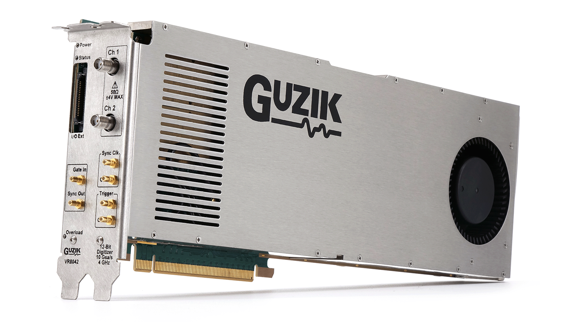
VR8042
4 GHz, 12-Bit Streaming Digitizer
Key Features
- 2 channels at 10 GSample/s
- DC to 4 GHz analog bandwidth
- 12-bit resolution
- 64 GByte of memory (5.15 seconds)
- 64 mV to 8 V input (45 calibrated ranges)
- 8.4 GSa/s streaming to CPU and storage
- Signal averaging with 99% trigger efficiency
- Real-Time Digital down converter
- Dedicated high-precision external trigger
Overview
The Guzik VR8042 is a 12-bit, 10 GSa/s digitizer that combines adjustable frontends, high-speed ADCs and built-in FPGA digital signal processing, which enables signal capture and analysis with high-throughput data transfer to host computer of up to 13 GByte/s. The VR8042 comes as a pluggable module in a 2U PCI Express form factor.
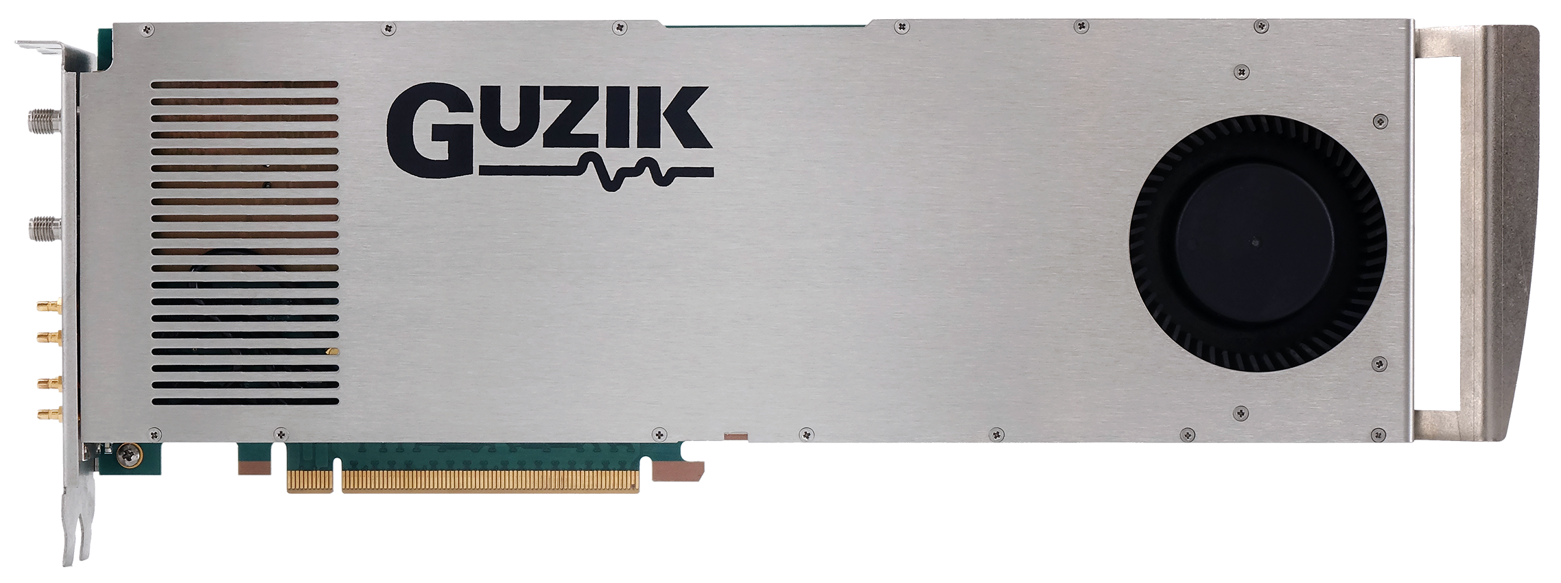
Figure 1. Guzik VR8042 digitizer
Front Panel
The front panel is shown in Figure 2. The following connectors are accessible on the front panel.
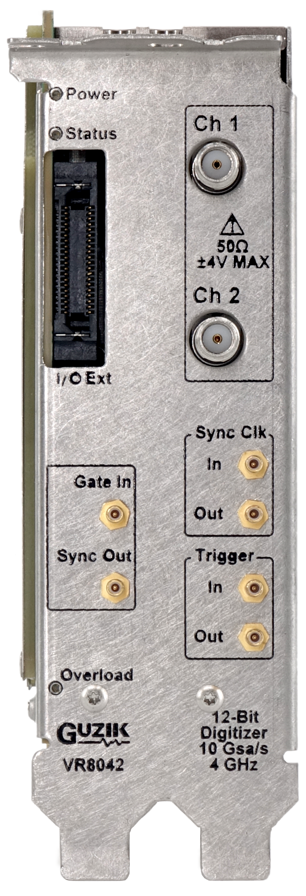
Figure 2. Front panel |
Ch 1, Ch 2 | Analog inputs of the digitizer, SMA connectors (field replaceable) |
| Sync Clk In | Reference signal input to synchronize internal OCXO-based clock generator, SSMB connector. The frequency of this signal is programmable from 10 MHz to 400 MHz and low phase noise is required. | |
| Sync Clk Out | 100 MHz clock for external devices synchronization. It can be used to synchronize other digitizers (in daisy chain mode), SSMB connector. | |
| Trigger In | External trigger input. This trigger should have low jitter and a slew rate ≥ 4 V/ns. The maximum frequency (for 100% trigger utilization) is 9 MHz. The trigger signal is converted to the digital domain and has jitter < 1 ps RMS. | |
| Trigger Out | Output signal to trigger external devices. It can be used for synchronization. | |
| Gate In | Control signal which can start acquisition. The maximum frequency is 100 MHz and is reclocked on a sub-harmonic of sampling frequency 10 GHz / 64 = 156.25 MHz. | |
| Sync Out | Output signal from FPGA for optional synchronization. | |
| I/O Ext | Reserved connector. | |
| LED Indicator | Power LED – solid green: normal. Can show under voltage or over voltage of digitizer power supplies
Overload LED – ADC overload, solid green is normal, solid red is overload. In case of overload the amplification is reduced to prevent ADC damage. The required amplification can be adjusted manually or automatically from Signal Display Control panel. Status LED – Solid green is normal. Red or orange indicates critical temperature or over temperature of digitizer components. For more information, see VR8042 Digitizer User’s Guide. |
Block Diagram
The VR8042 block diagram is shown in Figure 3.
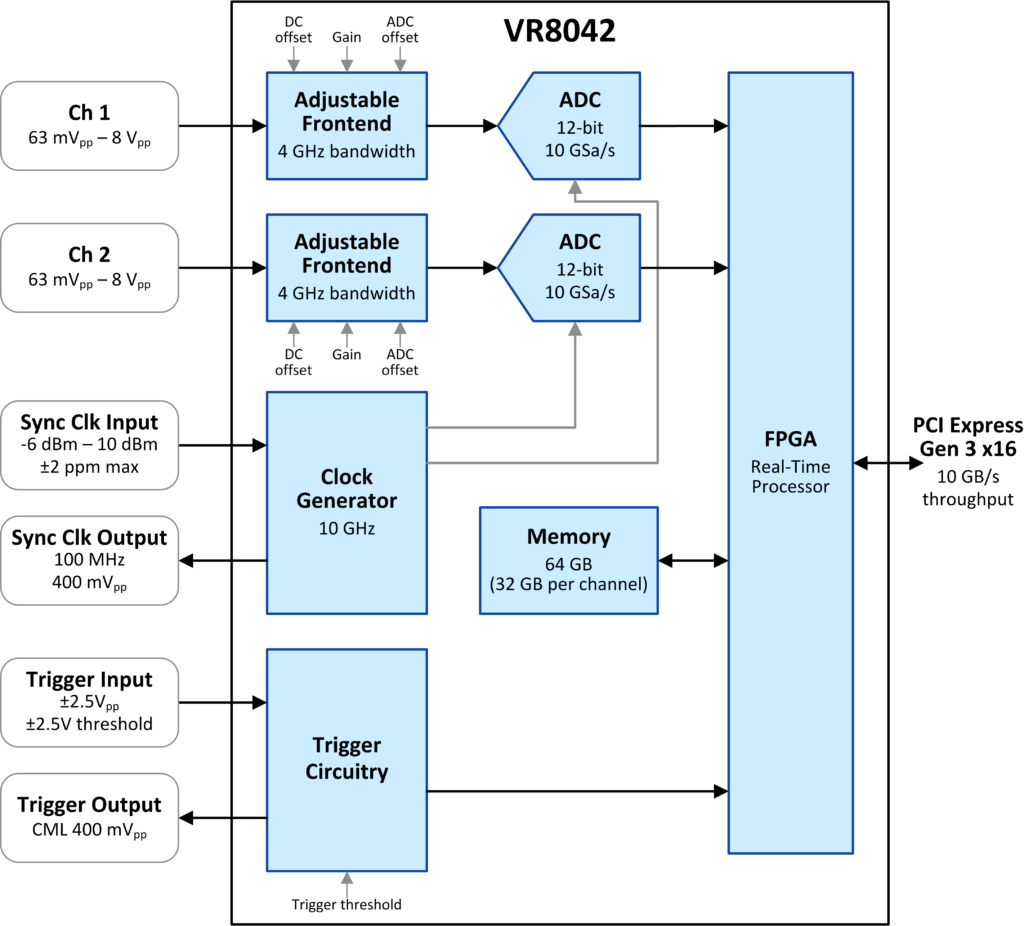
Figure 3. VR8042 block diagram
Adjustable Frontend
The adjustable frontend enables the digitizer to work with input signals in the range 64 mVpp to 8 Vpp (-20 dBm to +22 dBm) without external amplifiers or power dividers. Moreover, the wide range of DC offset adjustment allows the digitizer to work with maximum sensitivity in presence of DC voltage up to ±4 VDC. The gain of the frontend is calibrated with 1 dB steps. AC and DC coupling are available. The ADC offset can be adjusted to range ±0.5 of ADC full scale.
Synchronous Acquisition
Both channels are synchronized during signal acquisition: they use a common 10 GHz clock and share the same trigger. The skew between channels is calibrated to the value < ±5 ps for all channel sensitivities. Therefore, the channels can be used with different sensitivities while maintaining a skew < ±5 ps. Figure 4 shows the skew between channels vs sensitivity.
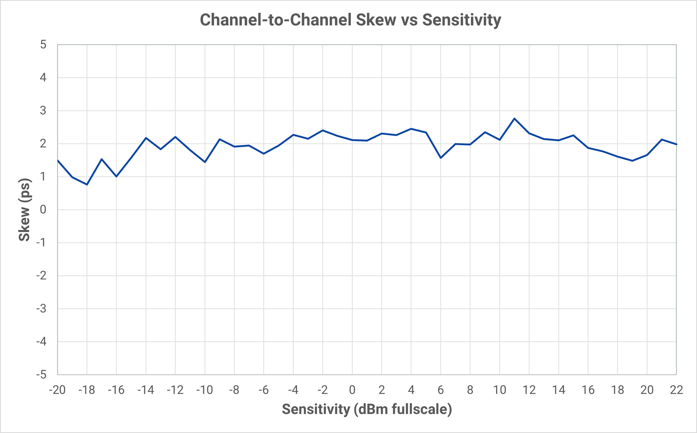
Figure 4. Channel-to-channel skew versus sensitivity
External Trigger
The external trigger (Trigger In) is converted to the digital domain and provides an accurate digitizer trigger with jitter < 1 ps. Additionally, the internal (channel) trigger can be used from any of the two analog input channels. The maximum frequency of the trigger is 9.16 MHz with 100% trigger utilization.
Clock Generator
The clock generator provides a 10 GHz clock for both ADCs. The clock is generated from an internal OCXO generator and can be synchronized by a reference signal connected to Sync Clk In. The external reference signal must have a frequency stability equal to or better than ±2 ppm.
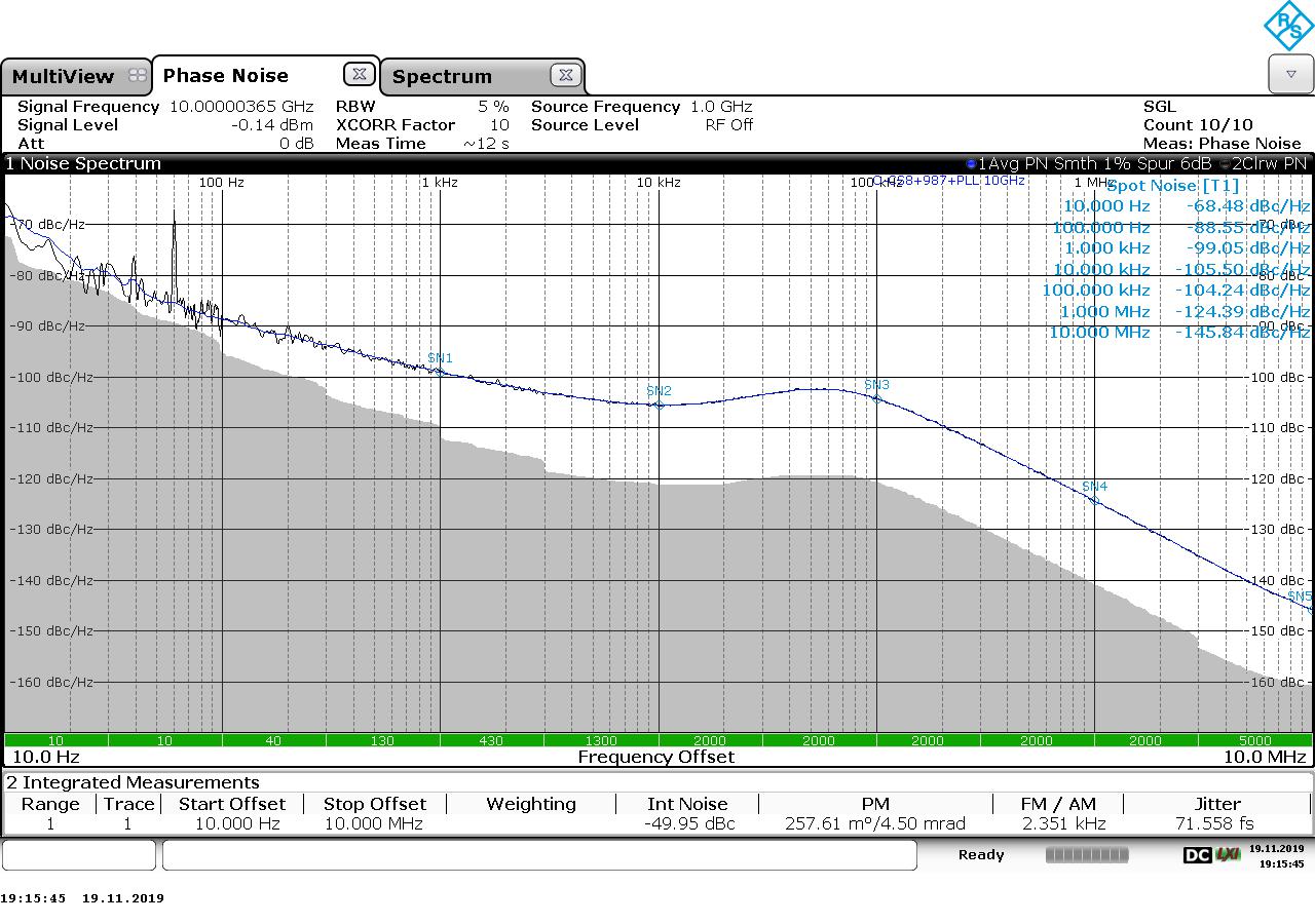
Figure 5. VR8042 10 GHz clock phase noise (spur suppression mode)
FPGA Real-Time Processing
The data from both ADCs is connected to an FPGA to perform real-time data processing. The FPGA is connected to 64 GB of memory (32 GB per channel) used for data storage and processing. Additionally, acquired and processed data can be transfer to the host computer through a PCI Express Gen 3 x16 interface with throughput up to 10 GByte/s.
Real-Time Equalization
Real-time equalization of amplitude frequency response and phase responses are performed for both channels. The equalization matches both responses to the target, a 6-pole Butterworth filter with linear phase response. The equalization is performed with input coax cables used to connect the digitizer’s analog signal inputs, Ch 1 and Ch 2. Note, cable delay is matched with an accuracy < 1 ps to achieve required skew between channels.
Real-Time Low-Pass Filtering and Decimation
Real-time low-pass filtering with adjustable bandwidth from 4 GHz and down to 62.5 MHz. When the filter cut-off frequency is reduced by twice or more, the corresponding decimation is applied. The entire frequency range uses decimations from 1 to 64 in powers of 2 for both channels. Filtering improves SNR and ENOB for signals with bandwidth below 4 GHz. Figure 6 shows the ENOB improvement for different decimation ratios. Additionally, filtering below 4 GHz results in data reduction, which requires less throughput to transfer the data to the host computer.
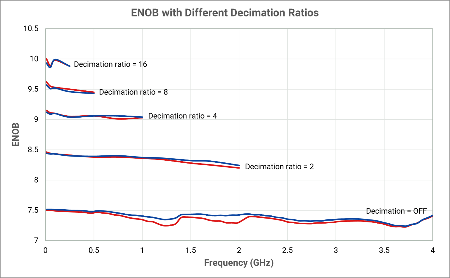
Figure 6. ENOB for channel 1 and 2 with different decimation ratios
Real-Time Data Streaming
Real-time data streaming continuously transfers data to the host computer RAM and stores to SSD. Streaming is available when using ADC or DDC modes. Streaming is necessary when required acquisition time exceeds the VR8042 onboard memory (32 GB = 2.57 seconds of acquisition time). When using a 4 TB SSD, the total acquisition time is extended to rough 4.4 minutes (102x longer acquisition time). The acquisition time can be further extended with decimation. VR8042 supports data streaming and storage to SSD with sustained speeds up to 10 GByte/s. The total amount of data transferred and stored is only limited by the SSD’s capacity. The VR8042’s onboard 64 GB memory is used as FIFOs to prevent data loss while streaming to the computer in the event of data transfer interruptions. There are three types of streaming: infinite streaming, segmented streaming and variable segmented streaming.
Infinite Streaming
A single trigger event starts the data streaming. ADC data is continuously streamed to the computer and stored to the SSD. Streaming ends when the SSD reaches capacity, or when the user manually initiates a stop. This type of streaming is used when a single extremely long or infinite measurement is performed.
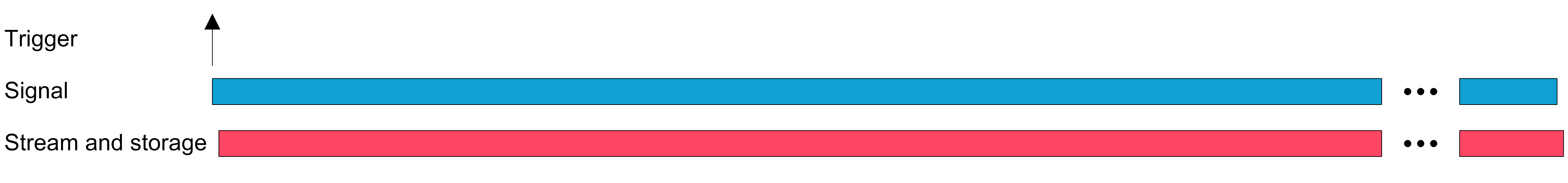
Figure 7. Infinite streaming
Each VR8042 channel has a sampling rate of 10 GSample/s, which is 15 GByte/s of continuous data. The maximum streaming and storage speed is 10 GByte/s. Therefore, real-time data streaming is achieved by performing decimation to reduce the sampling rate and amount of continuous data. For example, a single channel stream with decimation 2 has 7.5 GByte/s of continuous data. This can be streamed and stored in real time since it is below 10 GByte/s as shown in Figure 7. A dual channel stream with decimation 4 also has 7.5 GByte/s of continuous data, which can also be streamed and stored in real time as shown in Figure 8.
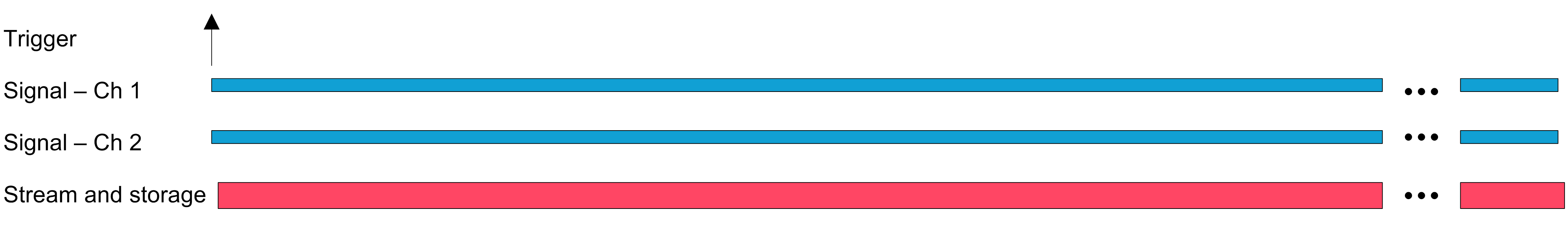
Figure 8. Infinite streaming with dual channels and decimation 4
Segmented Streaming
Multiple trigger events start the data streaming for each segment with fixed segment lengths. Segmented data is continuously streamed to the computer and stored to the SSD. The data in the gap between the end of one segment and the start of the next segment is not streamed or stored to the SSD. This is particularly useful when knowing beforehand that data in the gaps are undesirable, which conserves space on the SSD and alleviates transfer throughput speeds. There can be infinite number of segments until the SSD reaches its capacity or the user manually initiates a stop. This type of streaming is used for multiple segments while discarding undesirable data between each segment as shown in Figure 9.
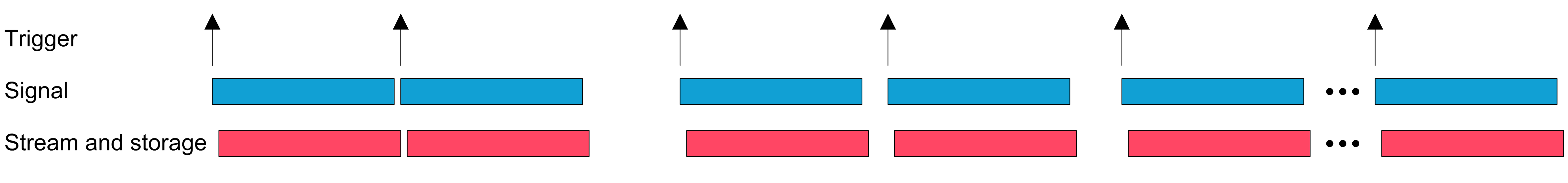
Figure 9. Segmented streaming
Full sampling rate streaming can be achieved when using segmented streaming with a sufficient gap between segments. The gap allows a segment streaming to complete prior to streaming the next segment. A single channel stream at full sampling rate has 15 GByte/s of continuous data. With a maximum streaming and storage speed of 10 GByte/s, the onboard FIFOs will reach capacity at one point. The gap allows the data in the FIFO to be completely streamed and stored to the SSD before starting the next segment. The duration of the gap is roughly half the segment length for a single channel stream as shown in Figure 10. A dual channel stream requires the gap to be roughly three times the segment length as shown in Figure 11.
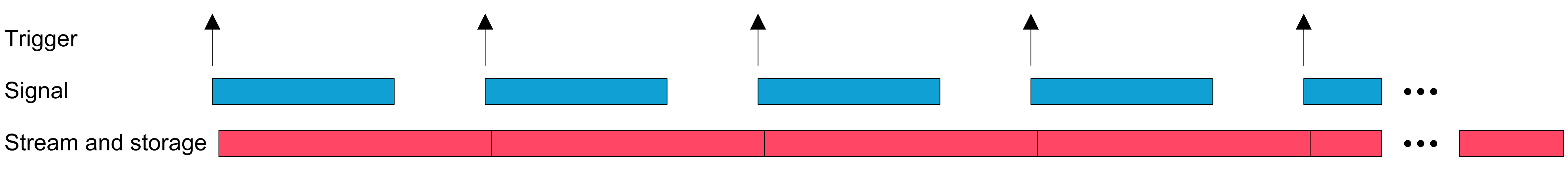
Figure 10. Segmented streaming of single channel with 10 GS/s sampling rate
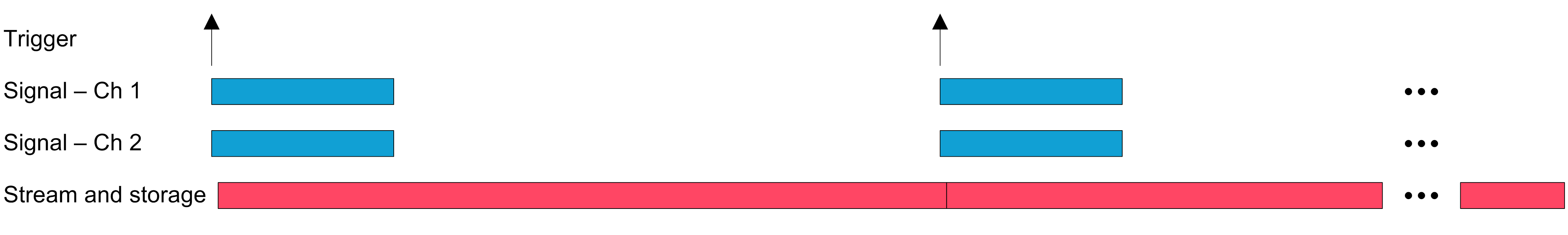
Figure 11. Segmented streaming of two channels with 10 GS/s sampling rate
Variable Segmented Streaming
A trigger event (start trigger) starts the data streaming with variable segment lengths. The start trigger indicates the start of a segment. The next proceeding trigger event (end trigger) indicates the end of the segment. The end trigger must occur after the minimum segment length. The next segment begins on the next trigger event (start trigger). Segment data is continuously streamed to the computer and stored to SSD. There can be infinite number of segments until SSD reaches capacity or the user manually initiates a stop. This type of streaming is used when multiple segments of variable segment lengths are performed and start (S) and end (E) triggers are provided as shown in Figure 12.
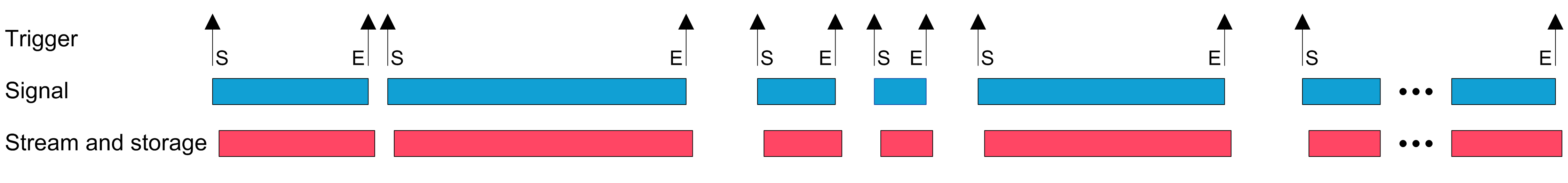
Figure 12. Variable segmented streaming with start and end triggers
Streaming Digital Down-Converter (DDC) Data
The real-time digital down-converter can stream and store its output to SSD in real time. Performing DDC with streaming is necessary for applications that require longer acquisition times that exceed the onboard memory. Streaming and storing to a 4 TB SSD extends DDC’s acquisition time from 3.4 seconds to roughly 6.8 minutes (107x longer). A single channel DDC data can be streamed and stored when specifying full span of 2 GHz or less. A dual channel DDC data can be streamed and stored when specifying a span of 1 GHz or less.
Streaming Data Format
The streaming data format is comprised of a stream header and data packets. At the beginning of each stream, there is a stream header that contains streaming meta information such as sampling rate, segment length, and vertical scale. After the stream header, data packets follow as shown in Figure 13. The stream header structure is described in Table 1. The streaming header size depends on the mode (ADC or DDC mode) and number of channels. For ADC mode, the header is 2304 bits wide for each dual channel streams and 4608 bits wide for single channel streams. For DDC mode, the header is 1024 bits wide for each dual channel streams and 2048 bits wide for single channel streams.

Figure 13. Streaming data format
Table 1. Stream header structure
| Offset | Size | Field Name | Description |
| 0 | 64 | Magic cookie | Unique sequence of bits that indicate the start of meta information section such as a header or footer.
ADC mode: DDC mode: |
| 64 | 8 | Stream version | Streaming data format version. |
| 72 | 2 | Meta information type | 0 – stream header 1 – data packet header 2 – data packet footer 3 – reserved |
| 74 | 22 | Reserved | Reserved. |
| 96 | 16 | Input sampling rate | The input sampling rate expressed in mega samples per second. |
| 112 | 8 | Decimation power | The decimation ratio expressed in power. (e.g., a value of 3 indicates 23 = 8 decimation ratio) |
| 120 | 64 | Sampling period | The sampling period expressed in femtoseconds. |
| 184 | 2 | Segment type | 0 – fixed segments 1 – variable segments 2 – infinite segment 3 – reserved |
| 186 | 1 | Infinite segment length | Use infinite segment length and overrides segment length. |
| 187 | 1 | Infinite number of segments | Use infinite number of segments and overrides number of segments. |
| 188 | 4 | Reserved |
Reserved. |
| 192 | 64 | Requested segment length | The requested segment length expressed in the number of samples. Only applicable for fixed segments. |
| 256 | 64 | Segment length | The segment length streamed expressed in the number of blocks. Only applicable for fixed segments. |
| 320 | 32 | Requested number of segments | The requested number of segments. |
| 352 | 16 | Block size | The number of bytes that define the granularity of sample grouping.
ADC mode: DDC mode: |
| 368 | 64 | Timestamp period | Timestamp period expressed in femtoseconds. |
| 432 | 64 | Vertical scale | Vertical scale in mV/bit expressed in 64-bit floating point. |
| 496 | 528 | Reserved | Reserved. |
| 1024 | 1024 | Reserved | Reserved. |
| 2048 | 256 | Reserved | Reserved. |
| 2304 | 2304 | Reserved | Reserved. |
Each ADC or DDC segment is stored in data packet that has its own header, payload and footer. The data packet header contains meta information such as segment start timestamp and trigger event timestamp. The payload contains the 12-bit ADC samples or 16-bit I and Q data from DDC. The footer contains the same information as the header with the addition of the segment length. This segment length is particularly useful after performing variable segmented streaming or when the stream has stopped prematurely. For ADC mode, headers and footers are 1152 bits wide for each dual channel streams and 2304 bits wide for single channel streams as show in Figure 14 and Figure 15. For DDC mode, the header and footers are 1024 bits wide for each dual channel streams and 2048 bits wide for single channel streams. The payload size depends on the streaming parameters. Table 2 shows the header and footer structure.

Figure 14. Data packet for each dual channel stream in ADC mode

Figure 15. Data packet for singe channel stream in ADC mode
Table 2. Data packet header and footer structure
| Offset | Size | Field Name | Description |
| 0 | 64 | Magic cookie | Unique sequence of bits that indicate the start of meta information section such as a header or footer.
ADC mode: DDC mode: |
| 64 | 8 | Stream version | Streaming data format version. |
| 72 | 2 | Meta information type | 0 – stream header 1 – data packet header 2 – data packet footer 3 – reserved |
| 74 | 22 | Reserved | Reserved. |
| 96 | 64 | Segment length | The segment length streamed expressed in the number of blocks. Refer to block size in the stream header. Only applicable in footer. |
| 160 | 64 | Data timestamp | Timestamp of the first sample in the segment expressed in number of timestamp periods after January 1, 1970 UTC. Refer to timestamp period in the steam header. |
| 224 | 32 | Data timestamp (fractional) | Fractional portion of timestamp of the first sample in the segment. Refer to timestamp period in the steam header. (e.g. 0x8000000 = 3.2 ns, when timestamp period is 6.4 ns) |
| 256 | 64 | Trigger event timestamp | Timestamp of the trigger event for the segment expressed in number of timestamp periods after January 1, 1970 UTC. Refer to timestamp period in the steam header. |
| 320 | 32 | Trigger event timestamp (fractional) | Fractional portion of timestamp of the trigger event for the segment. Refer to timestamp period in the steam header. (e.g. 0x8000000 = 3.2 ns, when timestamp period is 6.4 ns) |
| 352 | 672 | Reserved | Reserved. |
| 1024 | 128 | Reserved | Reserved. |
| 1152 | 896 | Reserved | Reserved. |
| 2048 | 256 | Reserved | Reserved. |
Real-Time Digital Down Converter (DDC)
Real-time digital down converter (DDC) with maximum span 2 GHz and binary decimation ratio 2 to 216 can be performed for both channels. The amplitude and phase frequency responses are equalized in real time to achieve accurate equalization in a narrow band of the DDC output signal. As a result, the DDC has an EVM = 1% with a real-time equalizer and 0.414% with software adaptive equalizer (in VSA software), see Figure 7.
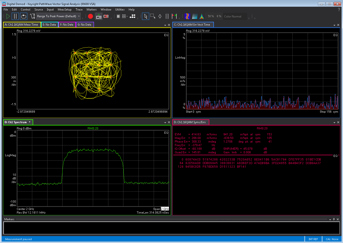
Figure 7. QAM16, 600 MBaud, 2 GHz span
The I/Q signals skew between channels is adjusted to be synchronous. The skew between I/Q signals is measured in degrees. Figure 8 shows the skew between the channels vs LO frequency. Figure 9 shows the skew between channels vs sensitivity. The typical skew value is < ±3 degrees.
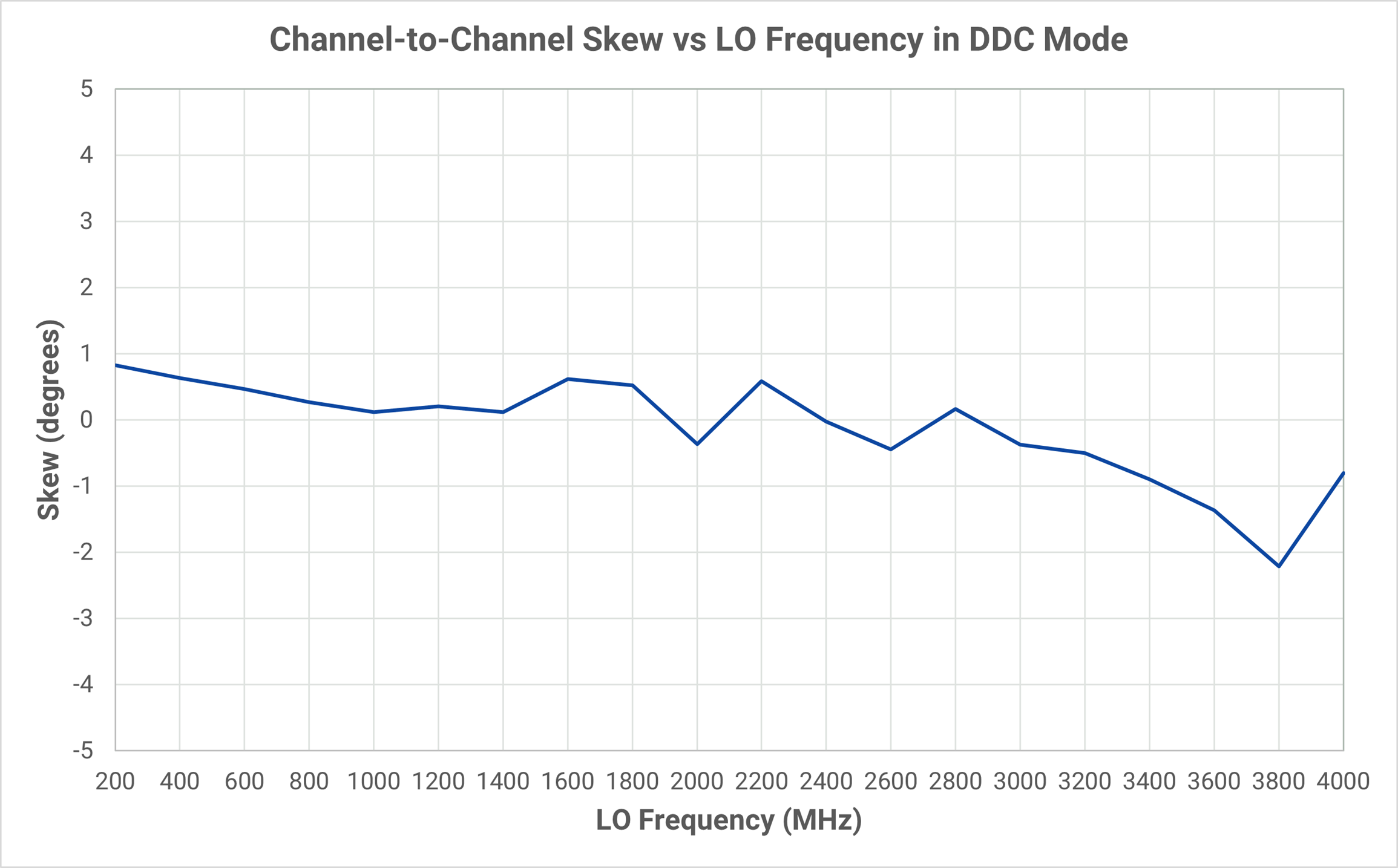 Figure 8. Channel-to-channel skew vs LO frequency in DDC mode
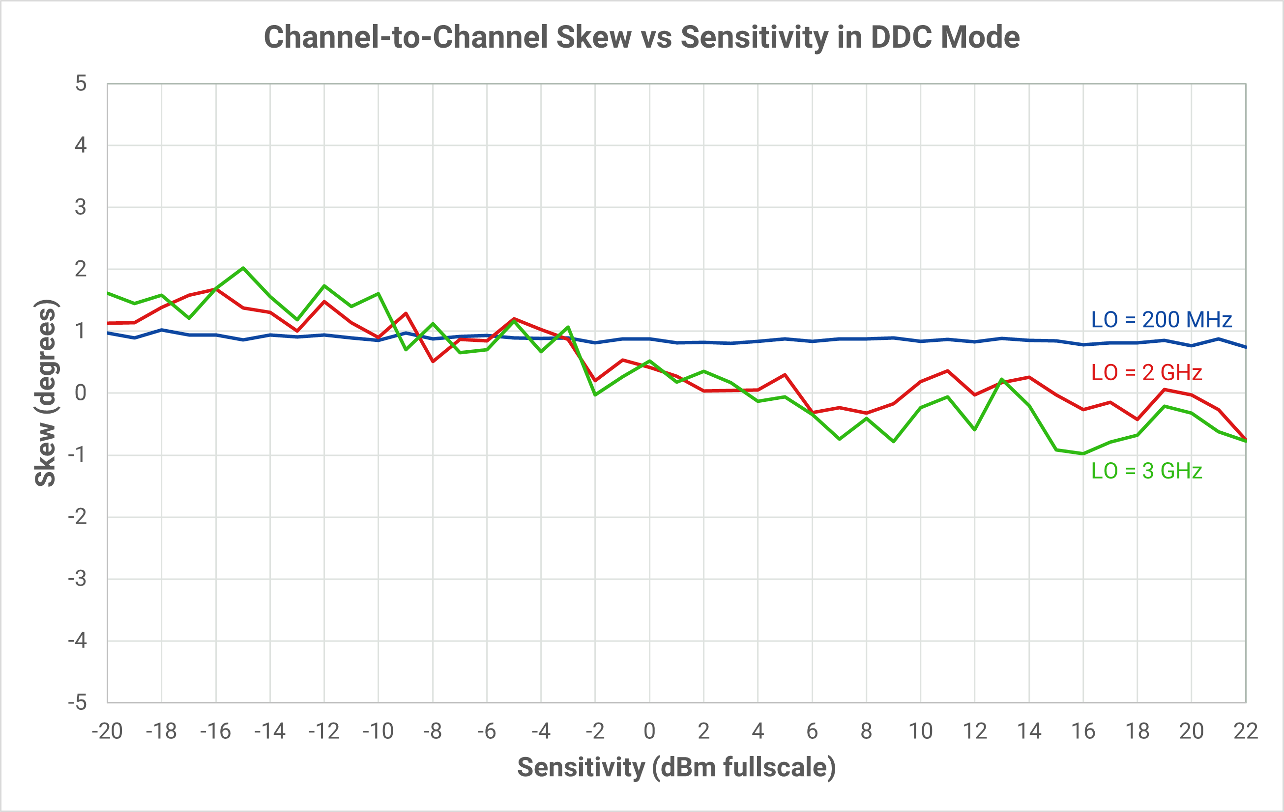
Figure 9. Channel-to-channel skew vs sensitivity in DDC mode
Real-Time Signal Averaging
The real-time signal averaging increases SNR of repetitive signals. The averaging uses an external trigger synchronous with the input signal. One averaging cycle increases SNR by 3 dB. An example of a signal detection heavily buried in noise using real-time signal averaging is show in Figure 10. The SNR of the input signal is -36 dB. The progression of averaging is demonstrated as a sequence of averaged waveforms with ten-fold average count increase from a waveform to a waveform. After 10,000,000 averages, the signal can be seen with an SNR of about 34 dB. 10 million averages were performed in 5 seconds using 2 MHz trigger repetition rate, delivering 99.9% trigger utilization.
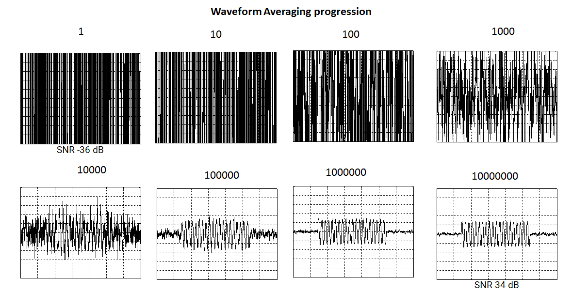
Figure 10. Real-time signal averaging at -36 dB SNR, showing progression of 10 million averages completed in 5 s
In certain applications, it is required to differentiate averaged waveform depending on additional external classifying signal. This mode requires that an extra signal be supplied to the gate input of VR8042, the classifying marker signal.
There are four classifying event modes:
- Off
Ignores the classifying events – the averaging works as usual with all segments accumulated. - Accept
An accumulation of a particular segment will only happen if a classifying event is detected. - Reject
An accumulation of a particular segment will only happen if a classifying event is not detected. - Classify
Allows you to separate accumulated segments based on classifying signal into different sub-accumulators. The classifying event is treated as a 1-bit number, so its absence results in an accumulation into sub-accumulator 0, and its presence into sub-accumulator 1. Figure 11 shows the timing diagram of the classifying marker operation in Classify mode.
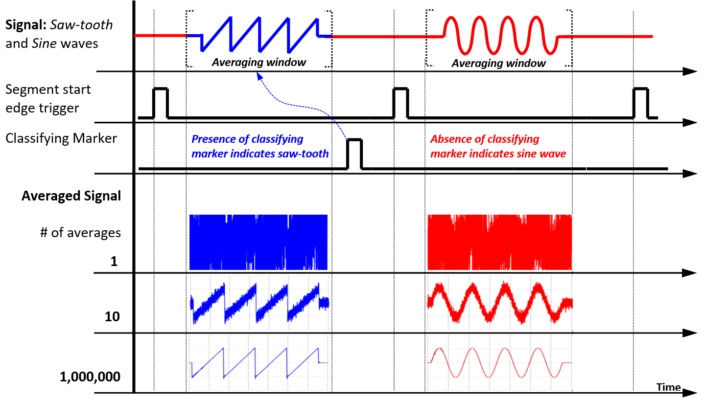
Figure 11. Classifying marker timing diagram
The input signal consists of two types of segments. The first type of segment (blue color) contains the saw-tooth signal. The classifying marker pulse is present within this type of segments. The second type of segment (red color) contains a sine-wave signal. The classifying marker pulse is absent within this type of segments. The Classify mode accumulates saw-tooth segments in one sub-accumulator, and sine-wave segments into another sub-accumulator, allow automatic separation of different types of signals into different accumulators.
For more details, refer to the Real-Time Signal Averaging with External Trigger application note.
https://www.guzik.com/product/real-time-signal-averaging-with-external-trigger/
SDK and Command Line Utilities
Custom software applications can be written to control the VR8042 using the GSA Software Development Kit (SDK). The SDK provides access to functions such as to initialize the hardware, acquire data, perform processing and transfer to host computer.
The GSA SDK API provides a set of functions exported from a Windows dynamic-link library (DLL). The API is declared in the C/C++ header (.h) file and alternatively in the type library (.tlb) file. The API can be used from C/C++ development environments such as Microsoft Visual C++ or National Instruments CVI by including the GSA SDK header file. This API can also be used with Microsoft .NET languages (C# and Visual Basic .NET) by referencing the GSA SDK type library. Additionally, the API can be used from the MATLAB language.
The GSA Toolkit includes several sample projects written in C++, C#, Visual Basic .NET and MATLAB.
Several of these C++ sample projects are included in GSA Toolkit’s installation as pre-compiled executable files. These projects can be used as a reference for customizing applications or to quickly and easily perform VR8042 measurements.
Signal Display
Signal Display is a graphical application that controls the VR8042 digitizer to observe input signals in time and frequency domains and perform acquisition of the signal. The software control panel has 4 display modes:
- Signal Display mode – to observe input signal in time domain (See Figure 12)
- Spectrum Display mode – to observe input signal in frequency domain (See Figure 13)
- DDC Display mode – to observe down converted signal in time domain (See Figure 14)
- DDC Spectrum Display mode – to observe down converted signal in frequency domain (See Figure 15)
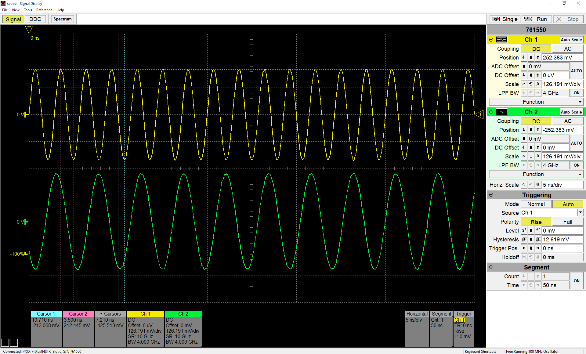
Figure 12. Signal (time domain) display with software control panel
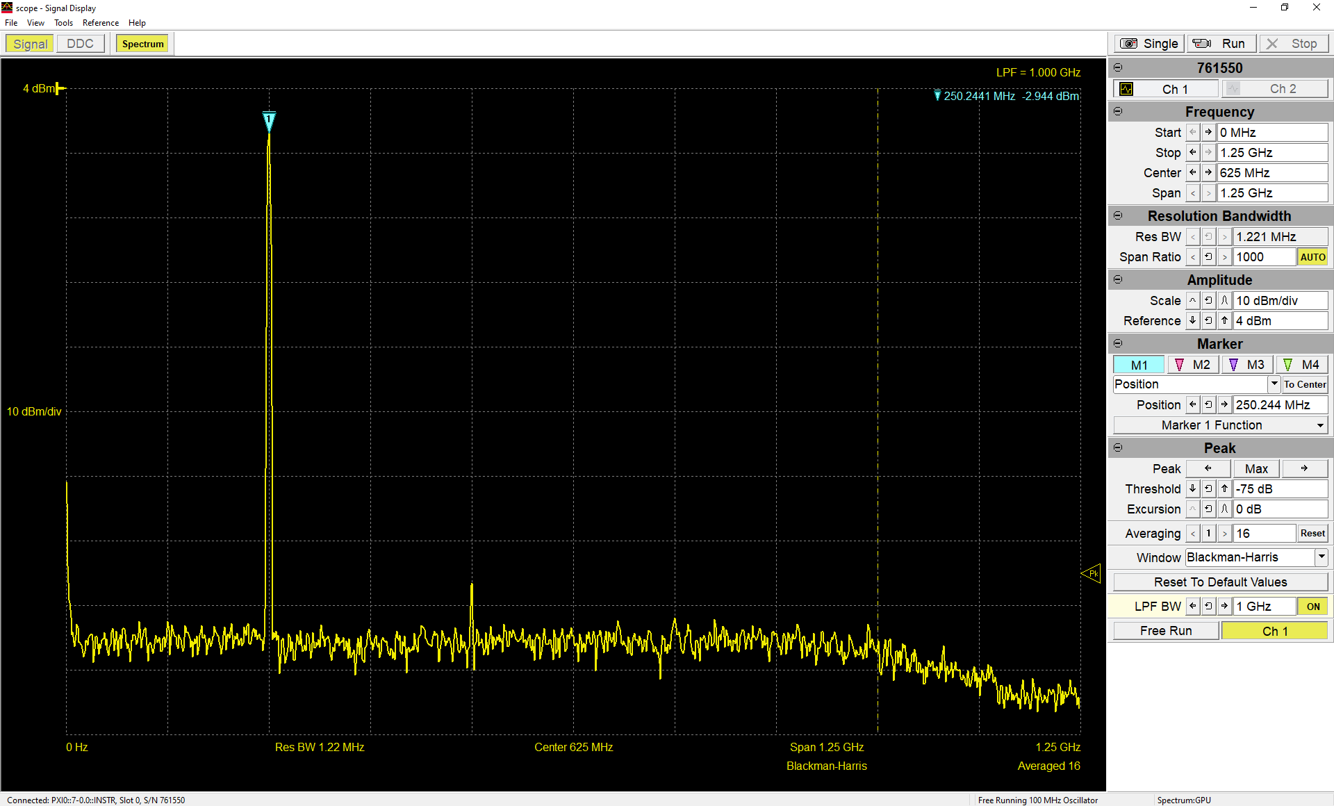
Figure 13. Spectrum analyzer (frequency domain) display with software control panel
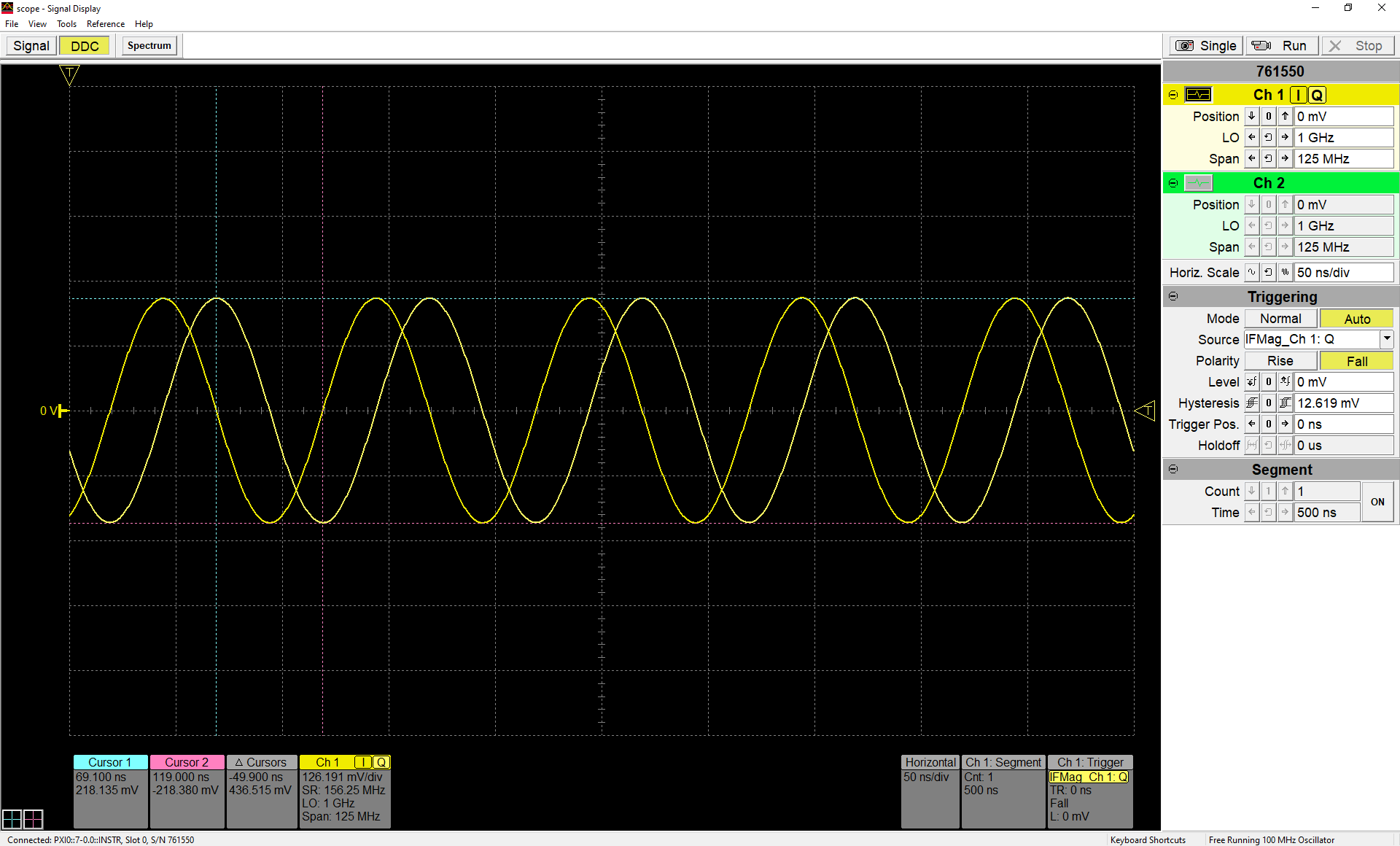
Figure 14. DDC signal (time domain) display with software control panel
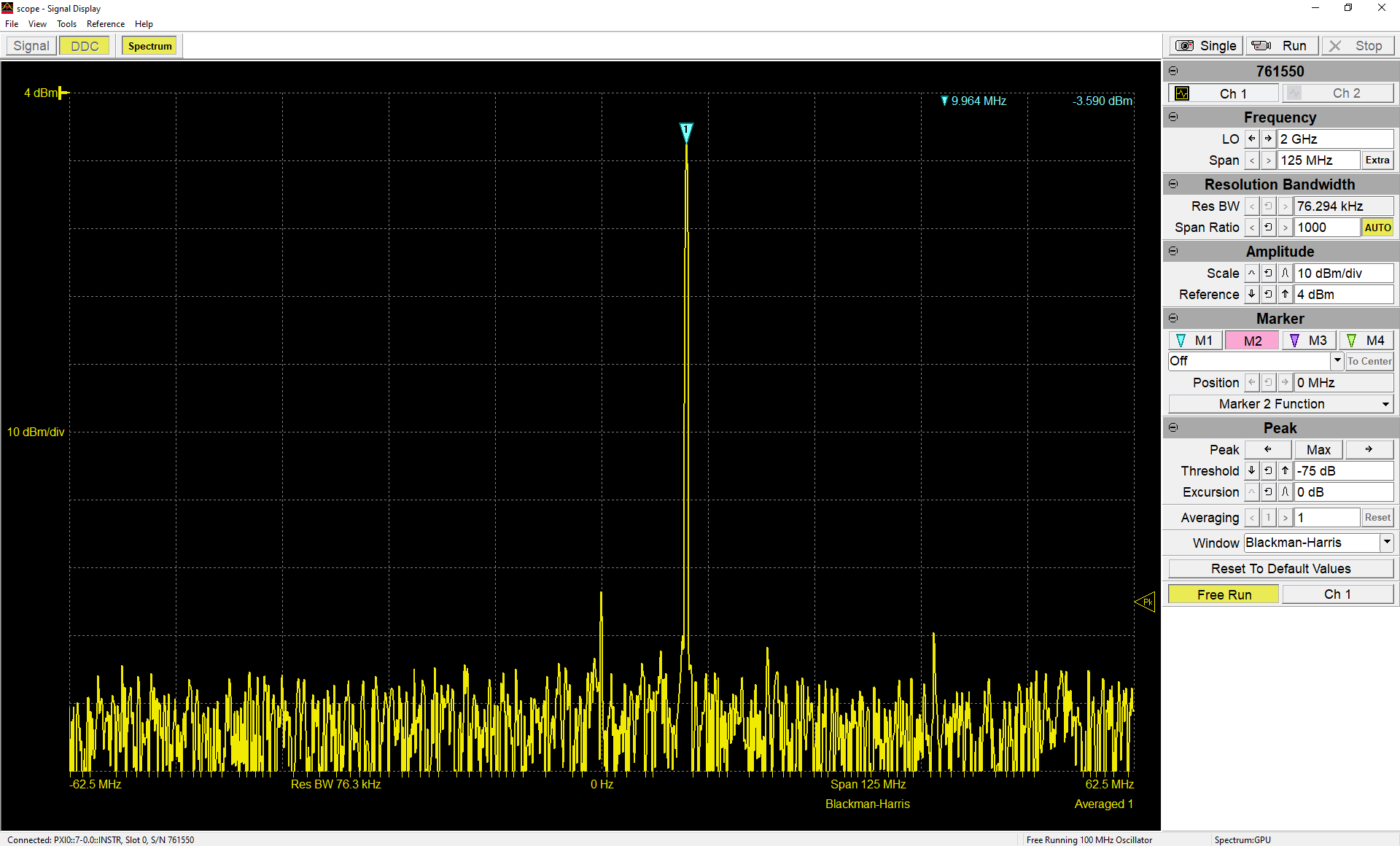
Figure 15. DDC spectrum analyzer (frequency domain) display with software control panel
Specification
Vertical System
| Number of channels | 2 |
| Input connector type | SMA |
| Maximum sampling rate | 10 GSa/s |
| Analog bandwidth (-3 dB)1,2 | DC … 4 GHz |
| Bandwidth flatness (-3 dBFS)1 | ±0.2 dB to 3.7 GHz |
| Vertical resolution | 12 bits |
| Input impedance | 50 Ω, 0.03 MHz … 4 GHz bandwidth DC: 115 Ω (typical) |
| Return loss (400 mV full scale) | 16 dB @ 100 MHz 22 dB @ 1 GHz 16 dB @ 2 GHz 16 dB @ 3 GHz 11 dB @ 4 GHz |
| Input coupling | DC AC (> 30 kHz) |
| Maximum input voltage | ±4 V |
| Input ranges | 64 mVpp … 8 Vpp (full scale) (-20 dBm … +22 dBm with 1 dB calibrated sensitivities) |
| Phase response to 4 GHz1 | ±1.5 deg |
| Effective number of bits (ENOB)1,3 (-3 dBFS, 400 mV full scale) |
7.50 @ 10 MHz 7.35 @ 1 GHz 7.30 @ 2 GHz |
| Effective number of bits (ENOB) with decimation1,3 (-3 dBFS, 400 mV full scale, see Figure 6) |
8.35 @ 1 GHz with decimation by 2 9.06 @ 0.5 GHz with decimation by 4 9.54 @ 0.25 GHz with decimation by 8 |
| Rise / fall time (10 – 90%) | 110 ps (measured) |
| SNR @ sensitivity (<2 GHz) | > 35.3 dB @ 64 mV full scale > 43.0 dB @ 200 mV full scale > 46.0 dB @ 400 mV … 8 V full scale |
| Spurious Free Dynamic Range (SFDR)1 (-3 dBFS, 400 mV full scale) (excluding in-band 2nd and 3rd harmonics) |
> 70 dBc @ 100 MHz > 70 dBc @ 1 GHz > 63 dBc @ 2 GHz > 60 dBc @ 4 GHz |
| Nonlinear distortions HD2 (-3 dBFS, 400 mV full scale) |
< -70 dBc @ 100 MHz < -65 dBc @ 1 GHz < -50 dBc @ 2 GHz |
| Nonlinear distortions HD3 (-3 dBFS, 400 mV full scale) |
< -70 dBc @ 100 MHz < -50 dBc @ 1 GHz < -48 dBc @ 2 GHz |
| Channel-to-channel skew (for all sensitivities, see Figure 4) |
< ±5 ps |
| Channel-to-channel isolation (two channels with equal sensitivity) |
70 dB @ 100 Mhz … 1 GHz 65 dB @ > 1 GHz |
| Gain accuracy (10 MHz) | ±3% (typical), ±4% (+5ºC to +35ºC) |
| Offset range (for all sensitivities) |
±4 V |
| Offset accuracy | ±2% (typical), ±2% ± 10 mV (+5ºC to +35ºC) |
| Offset resolution | 0.12 mV (nominal) |
Acquisition System
| Sampling rate (per channel) |
10 GSa/s |
| Single sideband (SSB) phase noise (10 GHz clock frequency) |
< -96 dBc/Hz (typical) at 1 kHz offset |
| Sampling clock jitter (10 Hz – 10 MHz) |
< 85 fs |
| Memory depth | 64 GB (32 GB per channel) |
| Data transfer throughput speed to computer | 10 GByte/s |
| Maximum acquisition time (per channel at maximum sampling rate) | 2.57 s (typical) |
Real-Time Data Streaming
| Data transfer speed | up to 10 GByte/s (sustainable) |
| Data transfer speed per channel | up to 5 GByte/s (dual channel stream) up to 10 GByte/s (single channel stream) |
| Maximum acquisition time (single channel segmented at 10 GS/s sampling rate storing to a 4 TB SSD) |
4.4 minutes |
| Maximum segment length | Infinite (254 samples when specifying a length) |
| Minimum segment length | ADC mode 19.2 ns x decimation ratio (dual channel stream) 38.4 ns x decimation ratio (single channel stream) DDC mode |
| Maximum number of segments | Infinite (226 – 1 when specifying number of segments) |
| Streaming data types | ADC mode 12-bit samples DDC mode |
| Stream header size | ADC mode 2304 bits (dual channel stream) 4608 bits (single channel stream) DDC mode |
| Data packet header and footer size | ADC mode 1152 bits (dual channel stream) 2304 bits (single channel stream) DDC mode |
| FIFO size | 32 GB per channel (dual channel stream) 64 GB (single channel stream) |
| Decimation ratios | ADC mode 1 … 64 DDC mode |
| Streaming types | Infinite streaming Segmented streaming Variable segmented streaming |
| Trigger source | External trigger Channel trigger Gate (Reclocked internally by 156.25 MHz clock synchronous with ADC sampling clock) Magnitude trigger (DDC mode only) |
| External trigger jitter4 | < 1 ps RMS |
| Channel trigger jitter4 | < 1 ps RMS (with interpolation) |
Real-Time Digital Down-Converter
| Maximum span | 2 GHz |
| DDC results data format | I (16-bit) and Q (16-bit) |
| Frequency response flatness | ±0.1 dB |
| Out of band attenuation (max span) | > 50 dB |
| EVM (2 GHz span, QAM 16, 600 MBaud) | < 1.1% |
| Channel skew (I/Q skew between channels) for different LO frequencies (see Figure 8) | < ±2.5 deg |
| Channel skew (I/Q skew between channels) for different sensitivities (see Figure 9) | < ±3 deg |
| Channel trigger types | I, Q, or magnitude |
DDC Decimation Ratio Configurations
| Complex (I/Q) Outputs | |||
| Decimation Ratio | Sample Rate, GSa/s | Bandwidth (span), GHz | SNR Improvement, dB |
| 4 | 2.5 (I) + 2.5 (Q) | 2 | 4 |
| 8 | 1.25 (I) + 1.25 (Q) | 1 | 7 |
| 16 | 0.625 (I) + 0.625 (Q) | 0.5 | 10 |
| 32 | 0.3125 (I) + 0.3125 (Q) | 0.25 | 13 |
| 64 | 0.1563 (I) + 0.1563 (Q) | 0.125 | 16 |
| 128 | 0.0781 (I) + 0.0781 (Q) | 0.0625 | 19 |
| … | … | … | … |
| 216 | 0.00015 (I) + 0.00015(Q) | 0.000122 | 46.2 |
Real-Time Signal Averaging
| Averaged waveform sample width | 64-bit floating point |
| Number of averages (per channel with max averaging window of 13 µs) |
67 million |
| Averaging window | Min: 12.8 ns Max: 13 µs 6.5 µs for 2 conditions of classifying marker |
| Averaging time (10 µs trigger period and 106 averages performed) |
100.7 s (100 s signal time) |
| Trigger: RMS jitter | ≤ 1 ps |
| Maximum trigger rate | 30 MHz |
| Rearm time | 12.8 ns |
| Trigger utilization | ≥ 99% |
| Pre-trigger range | 0 … 6.08 µs in 6.4 ns increments |
| Post-trigger range | 0 … 27.488 s in 6.4 ns increments |
| Classifying marker: number of conditions | 2 |
| Proximity to trigger | > 6.4 ns separation between trigger and classifying marker edges |
| Adjustment to trigger | -13 µs to 0.025 µs in 6.4 ns increments |
| Trigger-to-data alignment accuracy | better than 5 ps |
| Data transfer speed from digitizer | Up to 10 GByte/s |
Internal Time Base
| Frequency | 100 MHz (nominal) |
| Time base accuracy | ±50 ppb stability (v. Temperature 0ºC to 50ºC) + aging aging < ±2 ppm/10 years (maximum) aging < ±0.3 ppm/first year (typical) aging < ±5 ppb/day (typical) |
| Single sideband (SSB) phase noise | < -160 dBc/Hz (typical) at 1 kHz offset |
Channel Digital Trigger
| Edge trigger | Rising or falling edge |
| Frequency range | 0 … 4 GHz |
| Rearm time (deadtime) | 89.6 ns |
| Maximum trigger frequency5 (100% trigger utilization) |
9.16 MHz |
| Threshold adjustment | Full scale |
| Threshold resolution | 12-bit |
| Pre-trigger range | 6.45 us (typical) |
| Post-trigger range | 6.8 s (typical) |
| Hold-off time | 27.0 s (typical) |
| Trigger jitter4 | < 1 ps RMS |
External Trigger (Trigger In)
| Edge trigger | Rising or falling edge |
| Rearm time (deadtime) | 89.6 ns |
| Maximum trigger frequency5 (100% trigger utilization, pre-trigger ≥ 350 ns) |
9.16 MHz |
| Pre-trigger range | 6.45 us (typical) |
| Post-trigger range | 6.8 s (typical) |
| Hold-off time | 27.0 s (typical) |
| Trigger jitter | < 1 ps RMS |
| Front panel trigger connection | 1 SSMB female |
| Impedance | 50 Ω |
| Coupling | DC |
| Input range | ±2.5 V |
| Trigger threshold range | ±2.5 V |
| Threshold resolution | 0.1 mV (nominal) |
| Minimum pulse width | 150 ps TBD |
| Frequency range | up to 4GHz, 210MHz without pulses skipping |
| Hysteresis | 10 mV (typical) |
| Sensitivity | 100 mV at max frequency (30 mV at 10 MHz) |
| Slew rate | ≥ 4 V/ns for best jitter performance |
| Trigger jitter4 | < 1 ps RMS |
Trigger Output
| Front panel connector | 1 SSMB female |
| Impedance | 50 Ω |
| Common mode voltage | -200 mV |
| Level | CML, 400 mVpp |
| Coupling | DC |
| Rise / Fall Time (20 – 80%) | 120 ps |
| Delay to trigger input | 3 ns (typical) |
Reference Clock Input (Sync Clk In)
| Front panel connector | 1 SSMB female |
| Impedance | 50 Ω |
| Frequency | 10 MHz 20 MHz 25 MHz 50 MHz 100 MHz 200 MHz 400 MHz |
| Level | -6 dBm … +10 dBm |
| Coupling | AC |
| Slew rate | ≥ 4 V/ns for best jitter performance |
| Lock range | ±2 ppm (maximum) |
Reference Clock Output (Sync Clk Out)
| Front panel connector | 1 SSMB female |
| Impedance | 50 Ohm |
| Frequency | 100 MHz |
| Level | 400 mVpp (nominal) |
| Coupling | AC |
| Rise / Fall Time (20-80%) | 80 ps |
Synchronize Out (Sync Out)
| Front panel connector | 1 SSMB female |
| Impedance | 50 Ω |
| Level | 400 mVpp (nominal) |
| Coupling | AC |
Gate Input
| Front panel connector | 1 SSMB female |
| Impedance | 50 Ω |
| Input range | ±2.5 V |
| Coupling | DC |
| Minimum pulse width (100% utilization) | 6.4 ns |
| Threshold range | ±2.5 V |
| Hysteresis | 18 mV (typical) |
| Timing | Reclocked internally by 156.25 MHz clock synchronous with ADC sampling clock |
I/O External
| I/O External (IO Ext) | 1 Samtec ERF8-020 |
Host Computer
| Transfer Interface | PCI Express Gen 3 x16 |
| Operating System | 64-bit Windows 10 64-bit Windows 7 |
General Specifications
| Form factor | 2U PCI-Express full length |
| Dimensions (width x height x depth) | 41.91 x 126.5 x 352.3 mm 1.65 x 4.98 x 13.87 inches |
| Weight | 1.42 kg 3.13 lb |
| Power dissipation | 102 W |
| RoHS | EU/2015/863 |
| Operating temperature range | +5ºC to +35ºC (Limited by computer max temperature) |
| Non-operating temperature | -40ºC to +70ºC |
| Operating humidity | 5% to 80% relative humidity, non-condensing |
| Operating altitude | Up to 4,000 meters (12,000 feet) |
| Non-operating altitude | Up to 15,300 meters (50,000 feet) |
| Calibration interval | 1 year recommended |
1 With digital equalization
2 6-pole Butterworth approximation
3 ENOB is calculated as the following:
4 Low phase noise signal, slew rate > 4V/ns
5 The maximum trigger frequency is calculated as the following:
All specifications are subjected to changes without notice.
VR8042 Digitizer Licenses
| License | Description |
| Digitizer Base ADC_BASE |
Base license to use the VR8042 digitizer including single segment acquisition with real-time digital equalization of frequency and phase response of the digitizer, and data transfer to host computer. Total onboard memory is 64 GB (32 GB per channel). This license includes access to Guzik’s Software Development Kit (SDK) and a software control panel named Signal Display. |
| Segmented Memory Acquisition ADC_SM |
Acquire multiple fixed length segments by triggering on events with a minimum rearm time of 89.6 ns. Each segment is stored to the onboard memory, then transferred to the host computer. In this mode, the maximum trigger frequency is 9.16 MHz with 100% trigger utilization. This is an option license for: |
| Real-Time Low-Pass Filtering and Decimation ADC_BB |
Real-time digital low-pass filter (LPF) is used to reduce the analog bandwidth of the digitizer. It has an adjustable bandwidth from 4 GHz down to 62.5 MHz. If the input signal bandwidth is lower than 4 GHz, then a filter with a lower cutoff frequency can be applied to improve SNR and ENOB. Since the cutoff frequency is lowered, decimation by powers of 2 is performed. Decimation reduces sampling rate, therefore reduces the data speed to store data to the onboard memory and to transfer data to the host computer. As a result of decimation, the acquisition time increases proportional to the decimation factor.
This is an option license for: |
| External Trigger ADC_PT |
The external trigger provides a precise triggering event from an external source. The external trigger is converted to the digital domain with jitter < 1 ps. The maximum frequency of the trigger is 9.16 MHz with 100% trigger utilization.
This is an option license for: |
| Real-Time Signal Averaging ADC_AVGA |
Averaging of a repetitive signal improves the signal-to-noise ratio and reveals small signals otherwise buried in noise. Averaging is performed in real time with an external trigger synchronous with signal source. To achieve precise averaging, the trigger has a low jitter of < 1 ps RMS. Averaging is performed for two channels or one channel using the same external trigger. The maximum averaging window per channel is 13 microseconds. The maximum number of averages is > 67 million.
For more information, refer to the Real-Time Signal Averaging with External Trigger application note, https://guzik.com/product/real-time-signal-averaging-with-external-trigger/. This is an option license for: |
| Classifying Marker for Real-Time Signal Averaging ADC_BTRIG |
Classifying marker for Real-Time Signal Averaging is used to differentiate averaged waveform depending on an additional external classifying marker signal. The classifying marker is used to excluded select segments from the averaging process or average different segments in separately.
For more information, refer to the Real-Time Signal Averaging with External Trigger application note, https://guzik.com/product/real-time-signal-averaging-with-external-trigger/. This is an option license for: |
| Real-Time Digital Down Converter ADC_ADDCRT1 |
Real-time digital down converter (DDC) with maximum span 2 GHz and binary decimation ratio 2 to 216 can be performed for one or both channels. The amplitude and phase frequency responses are equalized in real time in a narrow band of the DDC output signal. As a result, the DDC has an EVM = 1.1% with span 2 GHz. Real-time IF Magnitude, I and Q triggering can be used to trigger data capture and stored to the digitizer onboard memory.
This is an option license for: |
| Fast Fourier Transform with Graphics Card (GPU) ADC_FFT1 |
Perform Fast Fourier Transformation with graphics card (GPU). This enables the spectrum analysis (frequency domain) for ADC and DDC modes in Signal Display.
This is an option license for: |